Important Notice
The full Sub-GHz transceiver (the AX series) range of products from OnSemi have been discontinued, with end-of-life scheduled for december of 2022: Official Notice
This includes the transceiver used here, the AX5043, and all others from the same family, the AX5243 and the new AX5045 as well as the SoC (MCU+RF) versions of them, the AX8052F143 and the new AXM0F343.
This page focuses on explaining the basics of how to set up the AX5043 transceiver. Being a highly configurable and versatile transceiver it is also complex to set up properly. ON Semiconductor provides a program to calculate register values and set up the radio, the AX-RadioLAB, which can be downloaded from the software section of the AX5043 page if you set up an account.
This program is useful to check some settings and effects they have but is very laking. It is incomplete, not even all modulations are possible, laking for example AFSK and many other settings… Also it exports ALL register settings not only those that differ from the default, so filtering out which ones actually needed change is annoying and changing all register is maddening as there are so many!
More important then the program is to read the datasheet and programming manual. But even after that, or even just looking the first time at them it is very overwhelming seeing all the configurations needed, specially for the RX mode! Also some information is only available from there blog, like how to set up PSK Modulation.
In this page I’ll try to show the basic set up needed to get you going and using this transceiver. I use the configuration used for my VUHF Radio project as examples, with the following characteristics:
- Oscillator: XO/TXCO with 16 MHz
- RF Frequency: 145.895 MHz and 436.45 MHz
- Modulations: AFSK @ 1200 bits/s and (G)FSK/(G)MSK @ 9600 bits/s
- Framing/Encoding: HDLC/AX.25 compatible and G3RUH compatible for the FSK modulation
Although the page focuses on the AX5043, the explanations and set-up instructions can be used for the new AXM0F343 SoC (MCU+RF) which uses the AX5043 as the transceiver core, although with different register address mapping. It can also be applied to the new AX5045, which is almost identical to the AX5043 with some small changes/improvements and some registers have a different address.
The first thing to get the RF communication going is to set up the oscillator input and RF synthesizer. All RF frequency parameters of the transceiver depend on the oscillator frequency. This also means that all RF frequencies inherit the tolerances of the used oscillator, this is, if the oscillator has a 20ppm frequency tolerance so will all the frequencies derived from this clock.
Bellow is a Block diagram of the RF synthesizer, as best as I can understand it:
The first step is to set the $ F_{XTAL} $ signal. For this we need to set what kind of oscillator input is used, a crystal or an oscillator (XO or TCXO) and set the REFDIV value so that the frequency at the PD input is below 24.8 MHz. For a 16MHz XO/TCXO the the following registers need to be set:
| Register | Name | Value | Comment |
|---|---|---|---|
| 0xF10 | PERFTUNE16 | 0x04 | TCXO: 0x04; Crystal: > 43 MHz: 0x0D; < 43 MHz: 0x03 |
| 0xF11 | PERFTUNE17 | 0x00 | Crystal: 0x07; TCXO: 0x00 |
| 0xF35 | PERFTUNE53 | 0x10 | TXCO/Crystal: < 24.8 MHz (XTALDIV = 1); > 24.8 MHz (XTALDIV = 2) |
In the case a Crystal is used as the oscillator input, the crystal load capacitance needs also to be set. This is in contrast to most other ICs (MCU or other transceivers) that use a crystal as the frequency source where this load capacitance is added externally at the terminals of the crystal. The load capacitance is set with the XTALCAP (0x184) register using the following formula $ C_L = 8 pF + 0.5 pF * XTALCAP $.
A useful debug step now is to set the SYSCLK GPIO to output the $ F_{XTAL} $ signal to check if it was correctly configured and working. For this the PINFUNCSYSCLK (0x021) register has to be set to 0x04 to output $ F_{XTAL} $ or 0x04 + N to output $ F_{XTAL} \over 2^N $.
The next step is to select the desired RF center frequency. For this the VCO and PLL has to be configured. I’ll only show how to use the internal VCO. Even then there are many different settings for the PLL and VCO, depending in which range the selected frequency falls. We can group them and create 4 different ranges and respective settings:
| RF Range | VCO Inductor | RFDIV |
|---|---|---|
| 27MHz to 262 MHz | External | ON |
| 54MHz to 526 MHz | External | OFF |
| 400MHz to 525 MHz | Internal | ON |
| 800MHz to 1050 MHz | Internal | OFF |
To note here that for frequencies from 525 MHz to 800 MHz an external VCO is needed, this case will not be explained. The two cases that I’ll explain are for 145.895 MHz and 436.45 MHz. In case of 145.895 MHz the external inductor and the RFDIV off is used, for this the following registers need to be set:
| Register | Name | Value | Comment |
|---|---|---|---|
| 0xF34 | PERFTUNE52 | 0x08 | RFDIV OFF: 0x08; RFDIV ON: 0x28 |
| 0x032 | PLLVCODIV | 0x30 | Bit 2 (RFDIV): 0; OFF Bit 4 (VCOSEL): 1; Use internal VCO2 with external inductor Bit 5 (VCO2INT): 1; Use internal VCO2 with external inductor |
In case of 436.45 MHz using internal inductor and RFDIV on:
| Register | Name | Value | Comment |
|---|---|---|---|
| 0xF34 | PERFTUNE52 | 0x28 | RFDIV OFF: 0x08; RFDIV ON: 0x28 |
| 0x032 | PLLVCODIV | 0x04 | Bit 2 (RFDIV): 1; ON Bit 4 (VCOSEL): 0; Use internal VCO2 with internal inductor Bit 5 (VCO2INT): 0; Use internal VCO2 with internal inductor |
For a start I leave the PLL Loop Filter settings to the defaults, they work well enough. There are many parameters that can be tuned so starting small and simple is the best. The next step is now to actually set our center frequency, in default the FREQA (0x034-0x037) register is used for this so only this one will be set. The value set to this register is given by the formula:
$$ FREQA = { F_{Center} \over F_{XTAL} } * 2^{24} + { 1 \over 2 }. $$
For example to get a center frequency of 145.895 MHz the register needs to be set to 0x091E51EC, and for a center frequency of 436.45 MHz to 0x1B473334.
To note again that as these frequencies are derived from the main oscillator, so they inherit its tolerances and for certain applications this means that this register value need to be tuned. The center frequency tolerance can be calculated from the oscillators frequency tolerance using the following equation:
$$ \Delta F_{Center} = { OSC_{Tolerance}(ppm) \over 1000000 } * F_{Center} $$
Using the 16 MHz XO with 20ppm as an example, the frequency tolerance for the 145.895 MHz case is $ \pm 2918 Hz $ and increases to $ \pm 8729 Hz $ for the 436.45 MHz case. This shows that depending on the desired modulation characteristics, channel bandwidth, etc, this needs to be taken into account and if needed compensated for, either by calibration and/or changing the oscillator type to one with better tolerances like a TCXO. TCXO have a frequency tolerance of around 0.5 to 2.5 ppm, a 10 times improvement over a XO or crystal.
The final step is to calibrate/auto-range the synthesizer. For this set RNGSTART (bit 4) of register PLLRANGINGA (0x033) and monitor this bit until it resets, goes back to 0, signaling the end of the auto-ranging. To check if the center frequency was set, PLL/Synthesizer got a lock, the RNGERR (bit 5) of register PLLRANGINGA (0x033) can be checked for ranging error and/or the PLLLOCK (bit 6) for a PLL lock. With this the center RF frequency is set!
Setting up the TX path is one of the simpler parts of configuring this transceiver. The first thing is to set the desired modulation. This is done by setting the MODULATION (0x010) register, this register is shared between RX and TX. For AFSK the MODULATION register is set to 0x0A and for (G)MSK to 0x07.
Next we select the desired bitrate, this is set with the TXRATE registers (0x165-0x167) based on the following formula:
$$ TXRATE = { BITRATE \over F_{XTAL} } * 2^{24} + {1 \over 2 } $$
For AFSK-1200 we want a bitrate of 1200 bits/s so the register is programmed to 0x04EB and for (G)MSK-9600 we want a bitrate of 9600 bits/s so it is programmed to 0x2753.
Next we set frequency deviation with the FSKDEV (0x161-0x163) registers. For FSK modulations like (G)MSK or (G)FSK the value to program is obtained from the following formula:
$$ FSKDEV = { F_{Deviation} \over F_{XTAL} } * 2^{24} + {1 \over 2 } $$
The frequency deviation of a FM signal is often given in the form of the modulation index (m) which is the ratio of the frequency deviation to the modulating frequency:
$$ m = { F_{Deviation} \over F_{Modulation} } $$
In digital binary frequency modulation (BFSK) the bits are transmitted as two different frequencies, either $ F_{center} - F_{Deviation} $ or $ F_{center} + F_{Deviation} $ depending on the binary state 0 or 1. Here the $ F_{Modulation} $ is given as $ { {1 \over 2} * BITRATE } $. So for BFSK modulations the modulation index is:
$$ m = { F_{Deviation} \over {1 \over 2} * BITRATE } $$
Now we can take this equation and the one that gives us the value of the FSKDEV registers and rewrite the later as a function of the modulation index:
$$ FSKDEV = { { m * {1 \over 2} * BITRATE} \over F_{XTAL} } * 2^{24} + {1 \over 2 } $$
For a (G)MSK modulation @ 9600 bits/s, which has a modulation index of 0.5 (definition of MSK), the FSKDEV register is programmed to 0x09D5.
Now in case of AFSK this register has a slightly different definition:
$$ FSKDEV = { { 0.858785 * F_{Deviation} \over F_{XTAL} } * 2^{24} + {1 \over 2} } $$
The standard AFSK-1200 modulation uses a $ F_{Deviation} $ of 3 kHz, so the FSKDEV is programmed to 0x0A8E.
For AFSK another pair of register has to be set. Because AFSK is a double modulation we have to set the parameters for both stages of the modulation. The frequency deviation that we just set is the second modulation so next we have to set the first modulation. This is the one that transforms the bits into two audio tones, called the Space for the 0 bit and Mark for the 1 bit. The Space frequency, 0 bit tone, is set by the AFSKSPACE (0x110-0x111) registers and the Mark frequency, 1 bit tone, is set by the AFSKMARK (0x112-0x113). The equation to calculate this register values is the following:
$$ AFSK(SPACE/MARK) = { { F_{Space/Mark} * 2^{18} } \over F_{XTAL} } + { 1 \over 2} $$
So for the AFSK-1200 specification, where the Space frequency is 2200 Hz and the Mark frequency is 1200 Hz, these registers are programmed to 0x25 and 0x14 respectively.
For the phase modulation, (B)PSK, the above frequency deviation settings are not relevant. The (B)PSK Modulation is controlled by the MODCFGP (0xF5F). This is NOT mentioned in neither the datasheet nor the programing manual, it is only mentioned in a blog post from On Semiconductors… With the registers bits having the following meaning:
| Bits | Name | Description |
|---|---|---|
| 2:0 | PSKPULSELEN | 000 : 1 001 : 2 010 : 4 011 : 8 100 : 16 101 : 32 110 : Invalid 111 : Off |
| 4:3 | PSKPULSEDFG | 00 : Positive 01 : Negative 10 : Copysign 11 : Invalid |
| 7:5 | PSKPULSEBOOST | 000 : 1 001 : 2 010 : 4 011 : 8 100 : 16 101 : 32 110 : 64 111 : Off |
The default of this register is 0xE7, disabling PSK. To enable PSK this register has to be modified, I used 0xE1 which worked well for BPSK @ 9600 bits/s.
Next we program the Frequency shape used. For a normal FSK or MSK modulation no frequency shaping is used and this step can be skipped as the default is using none. In case of GMSK, a Gaussian frequency shaping is used with a BT factor of either 0.5 or 0.3. This is set in the MODCFG (0x160) register with the following definition:
| Value | Meaning |
|---|---|
| 0x00 | No shaping or External Loop Filter |
| 0x01 | Invalid |
| 0x02 | Gaussian with BT = 0.3 |
| 0x03 | Gaussian with BT = 0.5 |
Finally the output power is set. Now it is possible to use a raised cosine amplitude shaping pre-distortion to the output signal but this will be ignored here. In this case the only register that needs do be modified is TXPWRCOEFFB which sets the output power, $ P_{OUT} $. The TXPWRCOEFFB is programmed to:
$$ TXPWRCOEFFB = { { P_{OUT} * 2^{12} - 1} \over P_{max} }, P_{max} = 16dBm $$
So to set the Output Power to the maximum of 16dBm, TXPWRCOEFFB is programmed to the following:
$$ TXPWRCOEFFB = { { 16 * 2^{12} - 1} \over 16 } = 4096 $$
And with this the analog TX path is programmed and ready to be used. There are many other registers that can be changed to improve performance or to achieve different modulation characteristics but for a start this is a good set-up. The next step is to program the RX path, or if only TX is desired the digital path, aka the framing.
This is by far the most complex part to set up. There are so many parameters/settings that can and need be adjusted that it is overwhelming at first, specially if one has never worked with a radio receiver. To try to explain better how the receiver parameters work and how to set them up I created the receiver block diagram as best as I understood it:
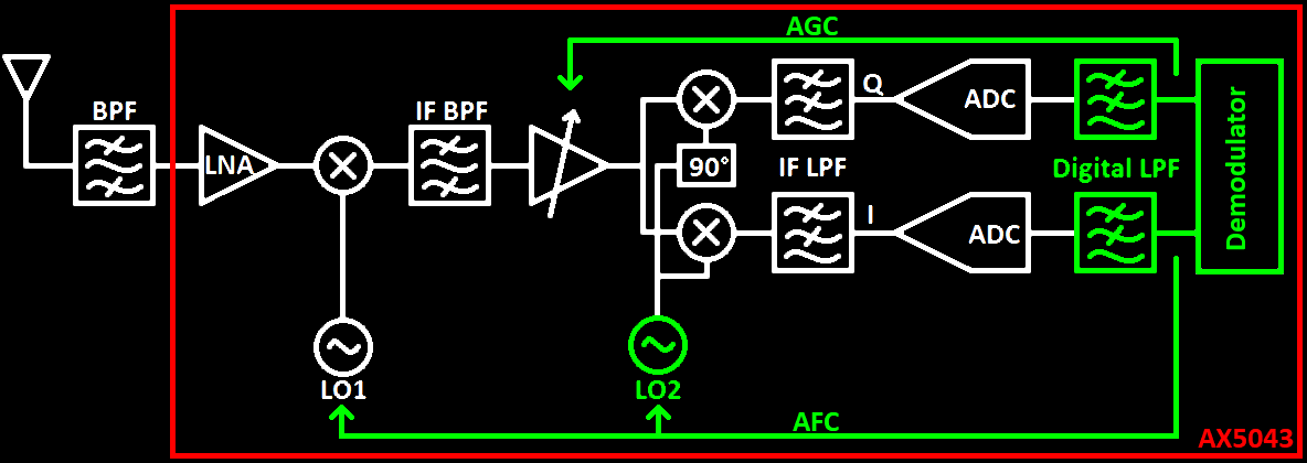
I’m not sure how accurate this actually is but it is good enough to help understand how to set up the receiver chain. The only blocks that can and need be adjusted are shown in green. The rest, as far as I understood, are fixed or set automatically by the radio. Important to note that both automatic gain control (AGC) and automatic frequency control (AFC) are based on the digitally filtered ADC output, so the receiving signal has to pass all previous filters and mixers for them to work properly.
As with the transmission, start by choosing the modulation. The modulation is set in the MODULATION (0x010) register, same as for reception. For AFSK the MODULATION register is set to 0x0A and for (G)MSK to 0x07.
The next step is to select the desired bitrate, which is controlled by the RXDATARATE (0x103-0x105) registers. Here the complication starts as the RXDATARATE register value depends on a register called DECIMATION (0x102) as can be seen by the equation that defines the RXDATARATE register
$$ RXDATARATE = { { 2^7 * F_{XTAL} } \over { F_{XTALDIV} * Bitrate * DECIMATION} } + {1 \over 2} $$
This means that to set the RXDATARATE register the DECIMATION register has to be set first. The DECIMATION register is what defines the digital LPF cutoff frequency. To set it the received signal bandwidth needs to be known so that it passes the digital LPF and can be demodulated properly. The receiver bandwidth depends on 3 factors:
- The Modulation selected
- The desired bitrate
- The desired AFC range
Starting with ignoring the AFC part and calculating the minimum receiver bandwidth needed to be able to demodulate the received signal. This is done by calculating the bandwidth a given modulation and bitrate combination occupies. For frequency modulations like (G)FSK and AFSK the required bandwidth is estimated by the Carson rule:
$$ BW = 2 * (F_{Deviation} + F_{Modulation}) $$
As seen in the TX section the $ F_{Modulation} $ for binary FSK is $ { {1 \over 2} * Bitrate } $ and the $ F_{Deviation} $ is $ {1 \over 2 } * m * F_{Bitrate} $, wih m being the modulation index. With this, and using the Carson rule, the bandwidth required for (G)FSK is
$$ BW = (1 + m) * F_{Bitrate} $$
So for (G)MSK modulation @ 9600 bits/s the required bandwidth is 14400 Hz, MSK is FSK with a m of 0.5.
For AFSK the Carson rule can also be used to calculate the bandwidth. As $ F_{Modulation} $ is the highest modulating frequency of the FM modulation, the second stage of the AFSK modulation, this is the space frequency (or mark if it is higher) used in the first stage of the AFSK modulation. The $ F_{Deviation} $ is the frequency deviation used for the second stage, the FM stage. Using AFSK-1200 as example, which has a mark frequency of 2200 Hz and $ F_{Deviation} $ of 3000 Hz, the required bandwidth is 10400 Hz.
The table bellow resumes the different equations used to calculate the minimum bandwidth for each modulation:
| Modulation | Bandwidth |
|---|---|
| (G)FSK/(G)MSK | $ (1 + m) * F_{Bitrate} $ |
| AFSK & FM | $ 2 * (F_{Deviation} + F_{Modulation}) $ |
| 4-FSK | $ (1 + 3 * m) * F_{Bitrate} $ |
| ASK | $ 1 * F_{Bitrate} $ |
| BPSK | $ 1 * F_{Bitrate} $ |
| QPSK | $ { 1 \over 2 } * F_{Bitrate} $ |
Now that the bandwidth required for each modulation is known, the minimum bandwidth that the digital LPF filter has to have is also known as it is the same. The digital LPF filter is set by the DECIMATION register, and by the FILTERIDX bits of the PHASEGAIN (0x126, 0x136, 0x146, 0x156) register and it’s cutoff frequency is defined by:
$$ BW = F_{coeff} * { F_{XTAL} \over {2^{16} * F_{XTALDIV} * DECIMATION} } $$
With $ F_{coeff} $ defined by the FILTERIDX bits of the PHASEGAIN register and its value given by in table bellow:
| FILTERIDX | -3dB BW | Nominal BW | -10dB BW | -40dB BW |
|---|---|---|---|---|
| 00 | 0.121399 | 0.150000 | 0.174805 | 0.256653 |
| 01 | 0.149475 | 0.177845 | 0.202759 | 0.284729 |
| 10 | 0.182373 | 0.210858 | 0.235718 | 0.317566 |
| 11 | 0.221497 | 0.250000 | 0.274780 | 0.356812 |
To simplify things ignore for now that there are multiple PHASEGAIN registers (4 of them) and set only the first one, PHASEGAIN0. Also admit that the FILTERIDX bits are set to 11, the default. With this the $ F_{coeff} $ value is 0.25, for the nominal bandwidth, and the DECIMATION register value can be calculated, defined by:
$$ DECIMATION = { F_{XTAL} \over {2^4 * F_{XTALDIV} * { 1 \over F_{coeff} } * BW } } $$
For AFSK-1200, the DECIMATION register is set to 0x18 and for (G)MSK-9600 to 0x11. And with this decimation value the RXDATARATE register is set to 0x0115C8 for AFSK-1200 and 0x3106 for (G)MSK-9600.
Next the $ F_{IF} $ is set. This sets indirectly the LO2 frequency from block diagram. The IF frequency is set by the IFFREQ (0x100-0x101) register and is given by
$$ IFFREQ = { { F_{IF} * F{XTALDIV} } \over F_{XTAL} } * 2^{20} + { 1 \over 2} $$
The $ F_{IF} $ is where the modulation spectrum will be centered around when sampled by the ADC and filtered by the digital LPF. So the $ F_{IF} $ needs to be high enough to nut cut-off the received signal spectrum either at DC (0 Hz) or at the digital LPF filter cut-off frequency, which is equal to its BW. Because of this the best seems to be setting the $ F_{IF} $ to be in the center of the digital LPF, $ F_{IF} = { BW \over 2 } $. For the AFSK-1200 case this is a $ F_{IF} $ of 5200 Hz and for (G)MSK-9600 of 7200 Hz, IFFREQ register set to 0x0155 and 0x01D8 respectively.
The next step is to setup the AFC loop. The AFC loop guaranties that the modulation frequency is tracked, so that if the received modulation deviates from the expected center frequency it is tracked and corrected. This also corrects offsets introduced by the receiver chain from not perfect LO synthesizer frequencies because of tolerances mainly of the reference clock. Here is where the tolerance of the oscillator used plays a major role.
Using the 16 MHz 20 ppm oscillator as example, we saw that for the 145.895 MHz case this gives a frequency tolerance of $ \pm 2918 Hz $. This means that for a radio link between two radios using this oscillator there is a frequency tolerance of up to $ \pm 2*2918 = 5836 Hz $. This because the emitter can emit, in the worst case, at $ F_{Center} = 145.895 MHz + 2918 Hz $ and the receiver expecting the center frequency being at $ F_{Center} = 145.895 MHz - 2918 Hz $. This means that for this worst case the AFC needs to be able to compensate for at least $ \pm 5836 Hz $. This increases to $ \pm 17.458 kHz $ in the case of 436.45 MHz.
The maximum RF frequency the AFC loop should tolerate/compensate is set by the MAXRFOFFSET (0x109-0x10B) register and is defined by:
$$ MAXRFOFFSET = { { \pm F_{Offset} } \over F_{XTAL} } * 2^{24} + {1 \over 2} $$
There is a limitation to how high this can be set as the received signal has to be able to pass the full RX chain, including the digital LPF, to be able to be tracked. This limits this range to about $ {1 \over 4} * BW $. This means for the 145.895 MHz AFSK-1200 case, with the already programed BW of 10400 Hz, the maximum AFC range is $ \pm 2600 Hz $ and for the 436.45 mhZ (G)MSK-9600 case it is $ \pm 3600 Hz $. This values are clearly below the calculated values needed for the AFC before, and therefore they may need to be increased to make the receiver work. For when the $ F_{Center} $, FREQA register, has been calibrated these values are good enough. If it needs indeed to be increased both the BW and IF frequency need to be adjusted to.
Keeping the BW and using the maximum possible AFC ranges, the MAXRFOFFSET register is set to 0x0AA7 for the 145.895 MHz and to 0x0EBF for the 436.45 MHz case. The MAXRFOFFSET register also sets if the frequency should be corrected at the first LO (bit 23 to 1) or the second (bit 23 to 0). I’m not sure what is better but doing it at the first LO seems more secure as this way the frequency is already correct when passing the IF band-pass filter (BPF).
Next is the set-up of the FSK deviation, but this can be skipped if the automatic mode is used, the recommended and default. This can always be set later to improve performance of the receiver.
For the AFSK case the space and mark frequency need to be set with there respective registers, AFSKSPACE (0x110-0x111) and AFSKMARK (0x112-0x113), which have a different definition in RX and TX mode. In RX mode the definition is:
$$ AFSK(SPACE/MARK) = { { F_{Space/Mark} * DECIMATION * F_{XTALDIV} * 2^{16} } \over F_{XTAL} } + { 1 \over 2} $$
So for the AFSK-1200 specification, with a space frequency of 2200 Hz and a mark frequency of 1200 Hz, the registers are programmed to 0xD9 and 0x76 respectively. The AFSK Detector Bandwidth also needs to be set with the AFSKCTRL (0x114) register. The value to be programmed is given by:
$$ AFSKCTRL = 2 * { log_2({ F_{XTAL} \over 2^5 * Bitrate * F_{XTALDIV} * DECIMATION }) } $$
With this the AFSKCTRL register has to be set to 0x08 for AFSK-1200.
The next step is to set up the AGC. First thing to set is the target ADC output magnitude, with the ADC being able to output values from 0 to 511 (9 bit ADC). This is done in the AGCTARGET (0x121, 0x131, 0x141, 0x151) register and, as with the PHASEGAIN register, ignore for now that there are 4 AGCTARGET registers and only set the first one, AGCTARGET0. The AGC target amplitude should be set close to the maximum ADC value, 512, to best use/fill the ADC range, but leaving a margin so that fluctuations do not to saturate the ADC. I use a value of around 0.75x of the maximum range, 384, as the target magnitude. Which based on the equation bellow
$$ AGCTARGET = log_2(Magnitude) * 16 $$
gives a value of 0x89 to be programed into the AGCTARGET register. Next the AGC hysteresis and minimum/maximum can be set, but for a start they can all be left at there default. What needs to be adjusted is the AGC loop speed, both the attack an release speed, controlled by the AGCGAIN (0x120, 0x130, 0x140, 0x150) register. The loop characteristic is given by the following equation:
$$ F_{3dB} = { F_{XTAL} \over 2^5 * \pi * F_{XTALDIV}} * ( 2^{-AGCATTACK} - 2^{-1-2*AGCATTACK} ) $$
with AGCATTACK being the lower 4 bits of the AGCGAIN register and can be substituted in the equation with AGCDECAY, the upper 4 bits of the AGCGAIN register, for the decay speed. The recommended AGCATTACK speed is $ F_{3dB} = Bitrate $ and the recommended AGCDECAY speed is $ F_{3dB} = { Bitrate \over 10 } $. To simplify the setting of this register value, all possible $ F_{3dB} $ values are shown in the table bellow and the closed one is selected:
| Value | $ F_{3dB} $ |
|---|---|
| 0x00 | 79577 |
| 0x01 | 59683 |
| 0x02 | 34815 |
| 0x03 | 18651 |
| 0x04 | 9636 |
| 0x05 | 4896 |
| 0x06 | 2467 |
| 0x07 | 1239 |
| 0x08 | 620 |
| 0x09 | 311 |
| 0x0A | 155 |
| 0x0B | 78 |
| 0x0C | 39 |
| 0x0D | 19 |
| 0x0E | 10 |
| 0x0F | 5 |
For AFSK-1200 this gives a AGCATTACK value of 0x07 and AGCDECAY of 0x0A, and for the (G)MSK-9600 this gives a AGCATTACK value of 0x04 and AGCDECAY of 0x07. With this the AGC loop is now set up. These values can of course all be tuned to improve AGC settling speed and demodulation sensitivity. To debug the AGC the AX5043 DAC can be set up to output the RSSI or SAMPLE_ROT_I/SAMPLE_ROT_Q, this is explained later.
The final step to get the receiver up and running is setting the timing gain recovery loop and datarate recovery loop. The timing gain recovery loop is set by the TIMEGAIN (0x124, 0x134, 0x144, 0x154) register and the datarate recovery loop by the DRGAIN (0x125, 0x135, 0x145, 0x155) register. The TIMEGAIN register is set according to the following equations:
$$ TIMEGAINxE = min | log_2({ Bitrate \over TMGCORRFRAC * 8 }) | $$ $$ TIMEGAINxM = max | { Bitrate \over TMGCORRFRAC * 2^{TIMEGAINxE} } | $$
With TIMEGAINxE being the 4 least significant bits of TIMEGAIN register and TIMEGAINxM the 4 most significant bits. TMGCORRFRAC should be a least 4, greater values reduce sampling jitter but slow down the timing lock-in. This means that for AFSK-1200 the TIMEGAINxE is set to 0x05 and a TIMEGAINxM to 0x09, when using a TMGCORRFRAC of 4. For the (G)MSK-9600 the TIMEGAINxE is set to 0x08 and TIMEGAINxM to 0x09.
The DRGAIN register is set according to the following equations:
$$ DRGAINxE = min | log_2({ Bitrate \over DRGCORRFRACx * 8 }) | $$ $$ DRGAINxM = max | { Bitrate \over DRGCORRFRAC * 2^{TIMEGAINxE} } | $$
With DRGAINxE being the 4 least significant bits of DRGAIN register and DRGAINxM the 4 most significant bits. DRGCORRFRAC should be a least 64, greater values reduce estimated datarate jitter but slow down datarate acquisition. This means that for AFSK-1200 the DRGAINxE is set to 0x01 and a DRGAINxM to 0x09, when using a DRGCORRFRAC of 64. For the (G)MSK-9600 the DRGAINxE is set to 0x04 and a DRGAINxM to 0x09.
Finally, it is recommended to set the FREQDEV (0x12C-0x12D, 0x13C-0x13D, 0x14C-0x14D, 0x15C-0x15D) to 0 so that the frequency offset estimator doesn’t lock at the wrong offset, whatever this means…
And with that the analog receiver path is configured and should work. For debugging the RX chain see the section about debugging the radio further down. With the receiver working based on these basic settings, more advanced features can be implemented and tuned to improve performance.
Advanced RX settings
TBD
The final step to get the radio up and running is to set up the packets/framing format. The first is to set up the encoding. Encoding happens between the framing unit and the modulator/demodulator and transforms, if enabled, the bit-stream. Different types of encoding can be used and combined. It is also possible to bypass both encoding and framing units and process all the raw bits in a MCU but I prefer to offload as much as possible to the transceiver.
For the 145.895 MHz AFSK-1200 example, using HDLC/AX.25, the encoder is set up according to these specifications. HDLC uses NRZI (Non-Return-to-Zero-Inverted) encoding and the AFSK-1200 mode doesn’t use a scrambler. Encoding is controlled by the ENCODING (0x011) register and for HDLC it needs to be set to 0x03, enabling differential encoding and bit inversion but not the scrambler.
For the 436.45 MHz FSK-9600 example, which is to be compatible with G3RUH the encoding, the same settings as with the AFSK-1200 mode are used with exception that it uses a scrambler. Luckily this transceiver has a scrambler with the correct polynomial, $ 1 + X^{12} + X^{17} $, used for G3RUH. So for this case the ENCODING register has to be set to 0x07, enabling differential encoding, bit inversion and the scrambler.
With encoding set it’s time to set up the framing. First set the framing mode to be used, in my case HDLC, which is done with the FRAMING (0x012) register. Here it can also be set if CRC check is to be used and which type of CRC. For HDLC it is enabled and set to use the CCITT 16-bit format/polynomial, $ X^{16} + X^{12} + X^{5} + 1 $ or 0x1021. For this the FRAMING register is set to 0x14, enabling HDLC frame mode and CRC check in CCITT 16-bit mode. Also the PERFTUNE114 (0xF72) register has to be set to 0x00, if frame mode is set to “Raw, Soft Bits” (0x01) this register has to be set to 0x06.
Next we have to set up how the packet is handled by the transceiver, like it’s length and possible address and patterns matching filtering. For AX.25 I leave all filtering disabled and enable arbitrary packet length. For arbitrary packet lengths, packet lengths are limited to 255 bytes if HDLC and CRC is handled in the transceiver, which is the case here, but the packets can be of any length below this limit. Arbitrary packet length needs to be used for AX.25 as it doesn’t have a length byte, frames are delimited by the HDLC flags (0x7E). For arbitrary packet lengths the following registers have to be set:
| Register | Name | Value | Comment |
|---|---|---|---|
| 0x201 | PKTLENCFG | 0xF0 | Bits 4:7 (LEN BITS): 0x0F |
| 0x203 | PKTMAXLEN | 0xFF | Set Maximum packet length |
| 0x233 | PKTACCEPTFLAGS | 0x20 | Bit 5 (LRGP): 0x01, Enable Accept Accept Packets that span multiple FIFO chunks |
With this the transceiver is now set up to be compatible with HDLC frames, so ready for AX.25. In this mode the transceiver is in charge of aligning all packets to the START Flags of the HDLC/AX.25 frame (0x7E) and also does the bit-stuffing process as well as CRC check. This means that the AX.25 frame assembling has to be handled in the MCU and no address check or filtering is done in the transceiver. This was done because the address filtering is only possible with up to a 32-bit address and a AX.25 frame address fields are 56 bits long. Now, it is probably possible to do a partial address checking in the transceiver but I have not implemented and tested this.
This section covers how to actually read and write frames/packets from and to the transceiver. And also how to set the operation mode, power mode, of the radio like TX and RX mode as well as what has to be changed when changing modes.
The main register that controls the Radio operation mode is the PWRMODE (0x002) register. This registers controls if the radio is in TX mode, RX mode, powered down, and many other different modes. The modes are controlled by the PWRMODE (0:3 bits) bits in this register. There are also bits to enable the internal reference circuit (bit 5) and the crystal oscillator circuitry (bit 6), which in normal operation need to stay enabled. With this the most important settings/modes for the PWRMODE register are:
| Name | Value | Comment |
|---|---|---|
| Powerdown | 0x60 | All circuits powered down |
| Standby | 0x65 | Crystal Oscillator enabled |
| FIFO Enabled | 0x67 | FIFO Enabled |
| RX Mode | 0x69 | Receiver Running |
| TX Mode | 0x6D | Transmitter Running |
Due to a Silicon Errata on the AX5043 Transceivers, listed here AX5043 ERRATA, a transition from RX to TX, and vice-versa, can’t be made directly as the FIFO is not correctly released this way. How these mode transition should be performed can be read in the errata and are also shown further down.
Reading and writing frame/packet data is done through the radio FIFO, attention to that the transceiver has to be in a power mode where the FIFO is enabled/powered which are all modes above and including “FIFO Enabled”. This transceiver has one shared FIFO with 256 bytes for both RX and TX. Because this FIFO can save many different types of data the data saved there is split into chunks with a header that indicates what the chunk is saving as well as how big it is. The header is always the first byte of a chunk. Because RX and TX data packets can be longer then the FIFO size of 256 bytes, they can be split into many chunks of smaller sizes so that each chunk fits into the FIFO. This maximum chunk size is set in the PKTCHUNKSIZE (0x230) register.
For the simplest operation, used here as example, the chunk size is set to the maximum (240 bytes) by setting the PKTCHUNKSIZE to 0x0D. So as long as RX or TX packets are smaller then this, and the FIFO is empty, the packets are not split into multiple chunks.
RX<->TX Mode Switch
As already mentioned it is not recommended to switch between RX and TX modes directly as the FIFO is not released correctly. The workaround to this problem is to switch to different modes in-between the RX to TX switch, or vice-versa. The errata document, and also what I tested and works, is to switch first to the Standby mode, then to the “FIFO Enabled” mode and then finally to either the RX or TX mode. Special attention is needed to make sure the transceiver actually switched to the Standby mode, this can be done by checking the SVMODEM (bit 3) of the POWSTAT (0x003) register, in Standby mode it should read “0”. The switch to Standby mode only occurs with the FIFO empty so it has to be cleared beforehand.
Send Packet
The first thing to do to send a packet is to change the operation/power mode of the transceiver to TX mode, following the recommendation given above when switching from RX to TX. If in AFSK mode the AFSKSPACE and AFSKMARK registers have to be changed/set to there TX settings/value. This is because these registers have a different definition for TX or RX mode. To set the transceiver into TX mode, the PWRMODE (0x002) register is set to 0x6D. To check if the transition to TX mode has finished, the SVMODEM (bit 3) of the POWSTAT (0x003) register can be monitored, when it goes high the transition is complete.
With the transceiver in TX mode a packet can now be sent. Before the actual bytes of a packet are sent a preamble should to be sent. The preamble can be any N bit sequence but for best performance it is recommended to send a pattern with many transitions, for example 0xAA or 0x55. The length of this preamble depends on RX settings, bit rates, frequency tolerances, etc… For this example I use 20 bytes of 0x55 as preamble.
As seen a before, commands to the radio are done by writing chunks to the FIFO, where the first written byte is the command identifier or FIFO chunk header. Attention to checking if the FIFO has enough free space for the preamble and data packet/chunk. This can be checked by reading the FIFOFREE0 (0x02D) and FIFOFREE1 (0x02C) registers. Another way to make sure there is space in the FIFO is to flush it with a “Clear FIFO” command. This is done by writing 0x03 (Clear FIFO Command) to the FIFOSTAT (0x028) register. Another point that needs attention is that if the “FIFO not empty” interrupt, or any other FIFO interrupt, is used and enabled, for example for RX mode, this will be triggered when writing to the FIFO and can lead to reading the just written data and therefore clearing it from the FIFO!
To send a preamble the TRANSMIT DATA command (0xE1) can be used, where all 20 bytes of the preamble have to be put into the FIFO, or to save FIFO space, the REPEATDATA command (0x62) can be used where the transceiver sends the passed byte N times. This is the recommended command for preambles. This transceiver also allows to add special bits/frame handling for each packet sent by setting bits in the control field (2nd byte). This allows, for example, to bypass the encoder (bit inversion, scrambler, etc) or to not use CRC on this part and is also used to allow the transmission of packets spanning multiple chunks. The control field bits have the following definition:
| Bit | Name | Comment |
|---|---|---|
| 0 | PKTSTART | If is the first Chuck of the full packet/frame to be transmitted |
| 1 | PKTEND | If is the last Chuck of the full packet/frame to be transmitted |
| 2 | RESIDUE | If data bits is not multiple of 8: In last byte sends bits bellow the most significant bit at 1 |
| 3 | NOCRC | Suppress CRC generation |
| 4 | RAW | Bypass Framing but not encoding |
| 5 | UNENC | Bypass Framing and encoding |
To send a preamble both framing and encoding should be bypassed, this way the preamble sequence (0x55 in this case) is sent as set and not changed. The RESIDUE bit can be ignored as long as only complete bytes are sent, only needs to be considered if for example 10 bits of preamble should be sent. Also, for the preamble CRC needs to be suppressed and both PKTSTART and PKTEND set to 0 because the preamble is not part of the actual packet/frame. With this, to transmit the 20 bytes 0x55 preamble using the REPEATDATA command, the following bytes have to be written to the FIFODATA (0x029) register:
| Byte | Value | Comment |
|---|---|---|
| 0 | 0x62 | FIFO Chuck Header: REPEATDATA Command |
| 1 | 0x18 | Control Field: How the bytes should be transmitted |
| 2 | 0x14 | Repeat Count |
| 3 | 0x55 | Byte to be sent Repeat Count times |
The next step is to transmit to the FIFO the actual packet/frame bytes. For this the TRANSMIT DATA command (0xE1) is used. This command also has the control field byte with the same definition for each bit as in the REPEATDATA command. For the TRANSMIT DATA command, normally, only the last two bits are relevant, as in normal operation encoding, framing and CRC are used on every sent packet/frame. As long as the frame/packet is smaller then the set maximum chunk size, here 240 bytes, the frame/packet can be sent in one chunk. If this is the case both PKTSTART and PKTEND bits have to be set to 1. As an example, sending a complete frame in one chunk consisting of 100 bytes the following bytes have to be transmitted to the FIFODATA (0x029) register:
| Byte | Value | Comment |
|---|---|---|
| 0 | 0xE1 | FIFO Chuck Header: DATA Command |
| 1 | 0x65 | Chunk Length: Bytes of the frame + 1 for the Control field byte |
| 2 | 0x03 | Control Field: How the bytes should be transmitted |
| 3 | data[0] | Frame/packet byte 0 |
| 4 | data[1] | Frame/packet byte 1 |
| 3+N | data[N] | Frame/packet byte 0 |
| 102 | data[99] | Frame/packet byte 99 |
The last thing to do is to send a FIFO commit command, only after that the transceiver start to transmit the bytes set in the FIFO. The FIFO commit command is sending 0x04 to the FIFOSTAT (0x028) register. To check if the packet has been transmitted the RADIOSTATE (0x01C) register can be monitored, during transmission this register will return either 0x06 (In TX) or 0x07 (In TX Tail). When RADIOSTATE register stops returning either of those values the transmission is complete and a new frame/packet can be sent or the transceiver can be put in RX mode or powered down.
In resume, to send a packet the necessary steps are:
- Possibly disable FIFO Interrupts if are enabled
- Possibly set Radio Power Mode to Standby followed by “FIFO Enabled”, if it was in RX mode.
- If AFSK Mode: Change AFSKSPACE and AFSKMARK registers
- Set Radio Power Mode to TX: Write 0x0D to PWRMODE (0x002) register
- Wait for Mode change completed: Read SVMODEM (bit 3) of the POWSTAT (0x003) register
- Write the preamble to the FIFO: Write [0x62; 0x18; 0x14; 0x55] to FIFODATA (0x029) register
- Write the packet to the FIFO: Write [0xE1; Packet Length + 1; 0x03; data[0];…; data[N]] to FIFODATA (0x029) register
- Write FIFO Commit Command: Write 0x04 to the FIFOSTAT (0x028) register
- Wait for TX complete: Read RADIOSTATE (0x01C) register, when not 0x06 or 0x07
- Change Radio Power Mode or sent another packet
- Possibly re-enable FIFO Interrupts
Receive Packet
To start receiving packets the transceiver has to be in RX mode, following the recommendation given above when switching from TX to RX. In case of using AFSK, the AFSKSPACE and AFSKMARK registers have to be set to there RX settings. To switch the transceiver to RX mode the PWRMODE (0x002) register have to be set to 0x69. For RX mode there is no need to check when the switch is complete.
With the transceiver in RX mode it will start filling valid received packets into the FIFO. Received packets have to match patterns and/or type of framing used to be considered valid. For the HDLC example, to be a valid packet, it has to be in between two HDLC flags (0x7E). Further filtering of what packets are considered valid and should be stored into the FIFO is controlled by the PKTACCEPTFLAGS (0x233) register. The default is the most strict filtering possible, by setting bits in the PKTACCEPTFLAGS this can be eased up. With the bits having the following definition:
| Bit | Name | Comment |
|---|---|---|
| 0 | ACCPT RESIDUE | Accept Packets with a non integral number of Bytes (HDLC mode only) |
| 1 | ACCPT ABRT | Accept aborted Packets: For HDLC if more then 7 consecutive ‘1’ bits are received, faulty bit stuffing |
| 2 | ACCPT CRCF | Accept Packets that fail CRC check |
| 3 | ACCPT ADDRF | Accept Packets that fail Address check |
| 4 | ACCPT SZF | Accept Packets that are too long |
| 5 | ACCPT LRGP | Accept Packets that span multiple FIFO chunks: Set for arbitrary packet lengths |
In normal operation only the LRGP bit should be set, for arbitrary packet length set before. For debugging, setting the CRCF flag can be useful so that partially correct packets, ones with faulty CRC, are allowed to be received.
To check if a new packet has been received, the interrupt pin can be set up to signal this or the FIFOCOUNT (0x02A-0x02B) register can be monitored to see if new data is available in the FIFO. Attention here if it is set to interrupt mode as writing to the FIFO, during sending a packet, triggers the interrupt! If there is new data to be read, a packet was received, FIFOCOUNT will be greater then 0 and that amount of bytes has to be read from the FIFODATA (0x029) register. As with when writing to the FIFO, the received bytes are not pure data but include a chunk header. For a received packet of length 100, which means that FIFOCOUNT returned 0x67, the read bytes from the FIFO should be as follows:
| Byte | Value | Comment |
|---|---|---|
| 0 | 0xE1 | FIFO Chuck Header: DATA Chunk |
| 1 | 0x65 | Chunk Length: Bytes of the frame + 1 for the Control field byte |
| 2 | 0x03 | Status flags: RX Packet Status |
| 3 | data[0] | Frame/packet byte 0 |
| 4 | data[1] | Frame/packet byte 1 |
| 3+N | data[N] | Frame/packet byte 0 |
| 102 | data[99] | Frame/packet byte 99 |
The status flag byte indicates which filtering have failed, in case PKTACCEPTFLAGS has been set to allow for packets with failed filtering to pass. It also indicates if this is the first and/or last chunk, for packets longer then the maximum chunk size allowed. The definition for each bit of this byte is:
| Bit | Name | Comment |
|---|---|---|
| 0 | PKTSTART | If is the first Chuck of the full packet/frame to be transmitted |
| 1 | PKTEND | If is the last Chuck of the full packet/frame to be transmitted |
| 2 | RESIDUE | If data bits is not multiple of 8 |
| 3 | CRCFAIL | CRC Check failed |
| 4 | ADDRFAIL | Address field check failed |
| 5 | SIZEFAIL | Size field check failed |
| 6 | ABORT | If packet was aborted: For HDLC if more then 7 consecutive ‘1’ bits are received, faulty bit stuffing |
For HDLC mode, no address or size check, with no exceptions set in the PKTACCEPTFLAGS and a packet smaller then the maximums allowed chunk size, this should always read 0x03. For this example, where the maximum chunk size was set to 240 bytes, all received packets smaller then 237 will fit in one chunk. With this we have now the received bytes of a packet. Any further filtering and decoding has to be done in the MCU.
In resume, to receive packets in polling mode the necessary steps are:
- If AFSK Mode: Change AFSKSPACE and AFSKMARK registers
- Set Radio Power Mode to RX: Write 0x09 to PWRMODE (0x002) register
- Monitor FIFO Count register: Read FIFOCOUNT (0x02A-0x02B) register
- Read FIFO: Read FIFOCOUNT bytes from FIFODATA (0x029) register
- Check the received status flag byte and length byte
RX Tracking Variables
The AX5043 transceiver has some very interesting tracking variables and GPIO outputs that can come very in handy for debugging. Registers that I found most useful for debugging are:
| Register | Name | Type | Comment |
|---|---|---|---|
| 0x040 | RSSI | int8_t | The received signal strength in dB, value of the register is Signed |
| 0x043 | AGCCOUNTER | uint8_t | The current Gain of the AGC, in 0.75 dB steps |
| 0x045-0x047 | TRKDATARATE | uint32_t | Current RX datarate estimation/tracking |
| 0x04D-0x04F | TRRFKFREQ | int32_t | Current RX RF Frequency deviation from the set central frequency |
| 0x118 | RXPARAMCURSET | uint8_t | Bits 2:3: Indicate which RX Parameter set is in use |
More important and interesting then those register is using the special output functionality of some GPIOs, like DAC output and demodulated bit and bit clock outputs.
Using the DAC
The AX5043 transceiver has an integrated DAC that allows for different variables to be output. I found this VERY useful for debugging! Now the DAC is not like a normal DAC in that it doesn’t output a constant voltage but a modulated signal that needs to be low-pass filtered to get the actual output. This can be achieved with a first order RC filter or better a second order one like in the figure bellow, where for the first order filter the Op-Amp is optional:
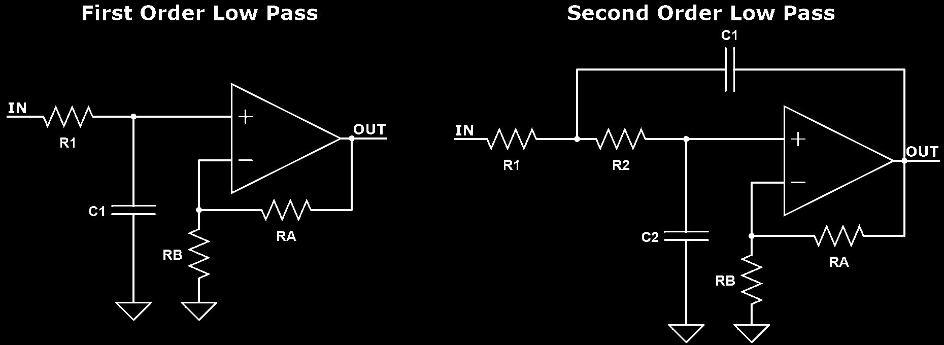
Two different modulation types are selectable, either $ \Sigma\Delta $ or PWM. $ \Sigma\Delta $ is recommended as PWM is only usable for low frequency outputs. In both mode the DAC resolution is 12 bits. In $ \Sigma\Delta $ the filtered output swing is from $ {1 \over 4 } * VDDIO $ to $ {3 \over 4 } * VDDIO $ and the frequency of the modulated signal is $ F_S = { F_{XTAL} \over 2 } = { 16 MHz \over 2 } = 8MHz $ in normal mode and double that if DACCLKX2 bit is set in the DACCONFIG (0x332) register. In PWM mode the filtered output swing is from $ {1 \over 4 } * VDDIO $ to $ {3 \over 4 } * VDDIO $ and the frequency of the modulated signal is $ F_S = { F_{XTAL} \over 2048 } = { 16 MHz \over 2048 } = 7.8 kHz $ in normal mode.
Many different signals can be used as inputs to the DAC, this is set by the DACINPUT bits of the DACCONFIG (0x332) register. As example on how to set up the DAC I’ll use the two signals I found most useful in the debugging process, the RSSI and the SAMPLE_ROT_I/SAMPLE_ROT_Q. For outputting the RSSI the DAC is set up to use the RSSI as its input, by setting the DACCONFIG register to 0x07.
Next the selected input has to be scaled/shifted to fit the 12 bits resolution of the DAC. The DAC input signals are left aligned to a 24 bit register so to get the full scale of any DAC input we have to shift this 12 bits to the right to fit the 12 bits of the DAC. For this we set the DACSHIFT bits in the DACVALUE registers (0x330-0x331) to 0x0C.
Now the GPIO to be used as the DAC output is selected, for this example I’ll use the PWRAMP pin. To use this pin as the output the PINFUNCPWRAMP (0x026) register has to be set to 0x05. And that’s it, now PWRAMP outputs the RSSI as an analog signal. To output any other possible variable only the DACINPUT bits of the DACCONFIG register has to be changed, for example to output SAMPLE_ROT_I they are set to 0x08.
Using DATA and DCLK pins
The other very interesting and useful feature of the AX5043 transceiver is the possibility to directly interface with the Modem part by reading/writing bits to/from it through a dedicated interface. The dedicated interface is composed of two GPIO lines, the bit clock line (DCLK) and the data line (DATA). This interface can be setup as either a slave like interface where the DCLK signal is input to the radio or as a master like interface where the radio outputs the DCLK signal. The later is easier to use and is what I will be describing.
There are different modes this interface can be setup, besides the master or salve setting, like using framing data, async mode, etc. I’ll use the lowest level one where the bits are input/output directly from the encoder part. This means that the bits still pass the encoder part of the modem but nothing else, no framing or HDLC bit stuffing. Therefore the encoder still needs to be setup properly using the ENCODING register or turned off by setting this register to 0x00.
To setup the interface both the DCLK and DATA pins need to be setup properly. The DCLK pin function is controlled by the PINFUNCDCLK (0x022) register and has to be set to 0x04, which enables the bit clock to be output on this pin in both TX and RX mode. The DATA pin function is controlled by the PINFUNCDATA (0x023) and has to be set to 0x04. In this mode the DATA pin outputs the received bits when in RX mode and reads the bits when in TX mode without the need to change the pin function when switching between RX or TX mode.
With this setup the transceiver will output the decoded bits as a continuous bit stream when in RX mode on the DATA pin, synchronized with the falling edge of the DCLK signal so it should be read on the rising edge. In TX mode the transceiver modulates and outputs in continuous what is presented to the DATA pin.
On of the best and most exciting features of the AX5043 transceiver is sadly hidden from the general public/costumer: a analog and digital output mode of the baseband I/Q signals! From other features of the transceiver, like outputting this I/Q signal through the DAC (but only one at a time) it is no big surprise that it has such a feature hidden away. It was finally made public in May 2021, in a forum post on the official OnSemi forum, but with no update to either the datasheet or the programming manual. This opens the door for creating a cheap Sub-GHz Software-Defined Radio (SDR) with the AX5043 as the programmable front-end.
That post gives basic instructions on how to enable these experimental features, as OnSemi calls them, of outputting the baseband I/Q signals either as a analog signal or through a digital interface, which they call DSPMode. These features make the AX5043 transceiver even more interesting and enable a whole new area to explore with off chip signal processing! I successfully tested both of these features, with instructions and results presented bellow.
Analog I/Q
The first, and simpler, way to access the baseband I/Q signals of the AX5043 is using the analog I/Q outputs, where the ADC pins of the transceiver (GPADC1 and GPADC2) are used to output the analog I/Q baseband signals. To enable this feature, two hidden registers must be programmed: the TMMUX (0xF02) and the BBDETECTOR (0xF46). Both registers are not documented in the programming manual, and their existence and meaning was only made available through the above mentioned forum post. From that we get that the TMBOX bits, the lower 3 bits, of the TMMUX (0xF02) register are responsible for the multiplexing of the ADC pins (GPADC1/2) and can be programmed to the following values:
| Value | Meaning |
|---|---|
| 0x00 | Unspecified |
| 0x01 | GPADC1: IREF10 NTST GPADC2: VREF .800 |
| 0x02 | GPADC1: ITEST OSC GPADC2: VDD REF |
| 0x03 | GPADC1: AUXP I GPADC2: AUXN I |
| 0x04 | GPADC1: AUXP Q GPADC2: AUSN Q |
| 0x05 | GPADC1: AUXP I GPADC2: AUXP Q |
| 0x06 | GPADC1: OUT DET I GPADC2: OUT DET Q |
| 0x07 | GPADC1: VDD REGS GPADC2: VDD MODEM |
To output the baseband I/Q signals on the GPADC1/2 pins, the TMMUX (0xF02) register must be programmed to 0x05. The other register that controls the analog I/Q mode is BBDETECTOR (0xF46), with the following meaning of its bits:
| Bits | Name | Description |
|---|---|---|
| 3:0 | AUX EN | Baseband Enable Filter Output on Detector/Auxiliary Bus |
| 4 | DET COMP EN | Baseband Enable Detector |
| 5 | DET BUF EN | Baseband Enable Detector Output Drive Amplifiers |
| 6 | BB COMP I | Baseband Comparator I |
| 7 | BB COMP Q | Baseband Comparator Q |
And according to the forum post it must be programmed to 0x08, with no additional information on what the other values and bits actually do.
With these two registers programmed accordingly, the baseband I/Q signal is now output on the GPADC1 (I samples) and GPADC2 (Q Samples) pins. The figure bellow shows the output signal for a none modulated carrier at the RF input with -90 dBm. The amplitude of the output signal is controlled by the AGC target value, set with the AGCTARGET (0x121, 0x131, 0x141, 0x151) register, and the frequency of the baseband signal will depend on the set IF frequency and AFC tracking.
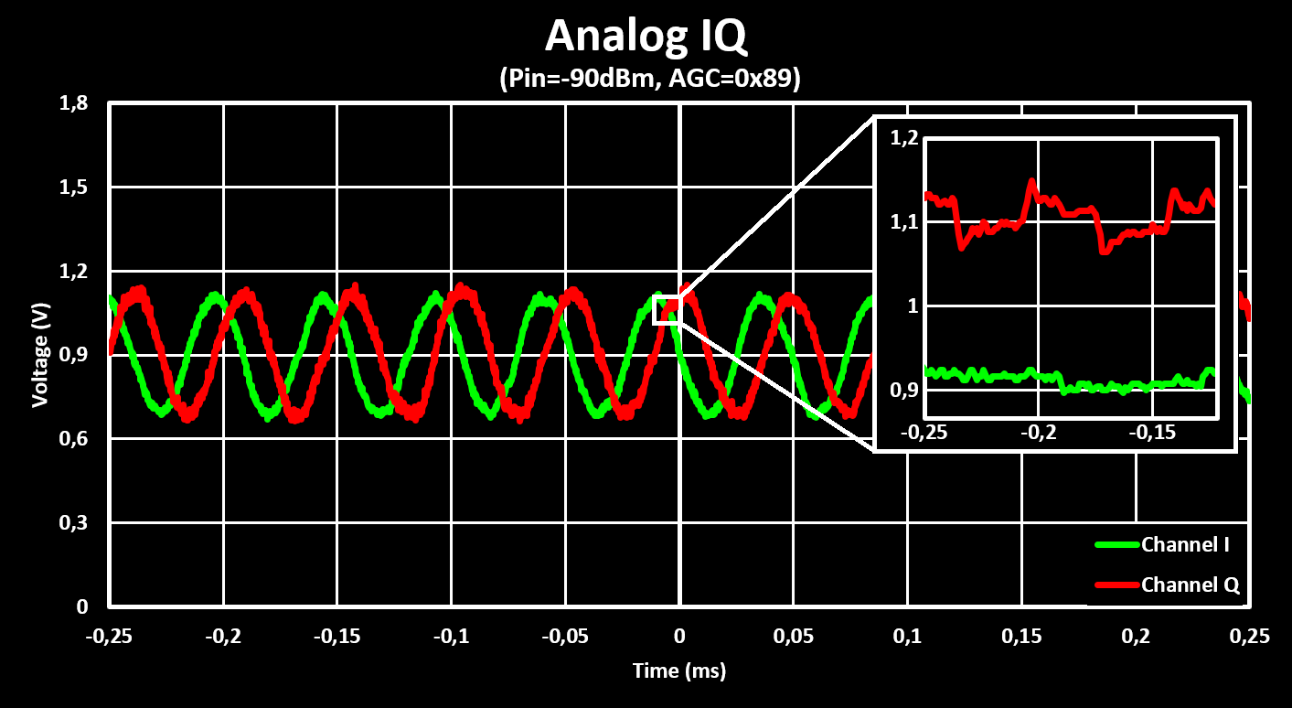
From the figure we can see that the analog baseband I/Q signal is quite noisy, and by zooming in it becomes evident that the majority of that noise comes from the input clock, here a 16 MHz TCXO. This is due to the close proximity of the GPADC1 and GPADC2 pins to the clock input (CLK16N/P) pins, they are side-by-side, and the layout of the used VUHFRadio module not being designed to minimize this interference doesn’t help either. This interference is made even more evident when comparing the interference level of the clock signal on the Q signal with the I signal, being much larger on the Q signal which is the pin closer to the clock input pins (CLK16N & CLK16P).
Digital I/Q
Although the analog baseband I/Q signals is a very cool feature, the much more exciting one is the digital I/Q mode, the so called DSPMode. This mode, as the name implies, is perfect to interface the AX5043 with a DSP where advanced digital signal processing can be implemented, like unsupported modulations. The AX5043 can even be programmed to output the baseband I/Q signals at different steps of the processing chain, or output any of the tracking variables. There are two ways of getting the digital I/Q signals, either reading them from a register over SPI or through a dedicated digital interface.
Starting with the interface/access of the data, in SPI mode the register DSPMODESHREG (0x06F) should be read to get the DSPMode frame bytes (access to the framing shift register), but the better and faster way is to use the dedicated digital interface. This interface uses the DATA, DCLK, PWRAMP (or ANTSEL) and SYSCLK pins, which will act as the RX bit output, frame sync, TX bit input, and bit clock input/output, respectively. To configure these pins, their respective control registers must be programmed (in the programming manual these are the “Invalid” functions):
- For DATA pin: Set PINFUNCDATA (0x23) register to 0x06
- For DCLK pin: Set PINFUNCDCLK (0x22) register to 0x06
- For PWRAMP pin: Set PINFUNCPWRAMP (0x26) to 0x06 and PINFUNCANTSEL (0x25) to 0x02, or vice-versa
- For SYSCLK pin: Set PINFUNCSYSCLK (0x21) to 0x04 if the AX5043 should output the bit-clock (can also be set as bit-clock input or to output lower bit-clock)
Now to actually enable, and set what data should be output in DSPMode, the following three hidden register must be programmed: DSPMODECFG (0x320), DSPMODESKIP1 (0x321) and DSPMODESKIP0 (0x322). The first configures the DSPMode interface, and has the following meaning for each bit:
| Bits | Name | Description |
|---|---|---|
| 1:0 | SYNCSOURCE | 00: Off; 01: Bit Clock; 10: Sample Clock; 11: Baseband Clock |
| 5:2 | NOT USED | |
| 6 | DSP SPI | Enable SPI shift register access |
| 7 | FSYNC DLY | 0: FSYNC set before first bit; 1: FSYNC with first bit |
The SYNCSOURCE bits set what signal is used to generate the frame sync (FSYNC) and must be selected according to what data will be output (what is the correct setting for each output data has to be guessed…). Also, if the SPI mode is to be used the DSP SPI bit must be set. What data is output, or written to the SPI shift register, is controlled by the DSPMODESKIP1 (0x321) and DSPMODESKIP0 (0x322) register. The DSPMODESKIP1 (0x321) register enables the skipping of the following data:
| Bits | Name | Description |
|---|---|---|
| 0 | SKIP FREQ | |
| 1 | SKIP PHASE | |
| 2 | SKIP DATARATE | |
| 3 | SKIP DEMOD | |
| 4 | SKIP AFSK DEMOD | |
| 5 | SKIP RSSI | |
| 6 | SKIP AGC | |
| 7 | NOT USED |
While the DSPMODESKIP0 (0x322) register enables the skipping of the remaining data:
| Bits | Name | Description |
|---|---|---|
| 0 | SKIP SOFT SAMP | |
| 1 | SKIP BASEBAND I/Q | |
| 2 | SKIP SAMP I/Q | |
| 3 | SKIP SAMP ROT I/Q | |
| 4 | SKIP SAMP MAG | |
| 5 | SKIP SAMP PHASE | |
| 6 | SKIP AMPL | |
| 7 | SKIP RF FREQ |
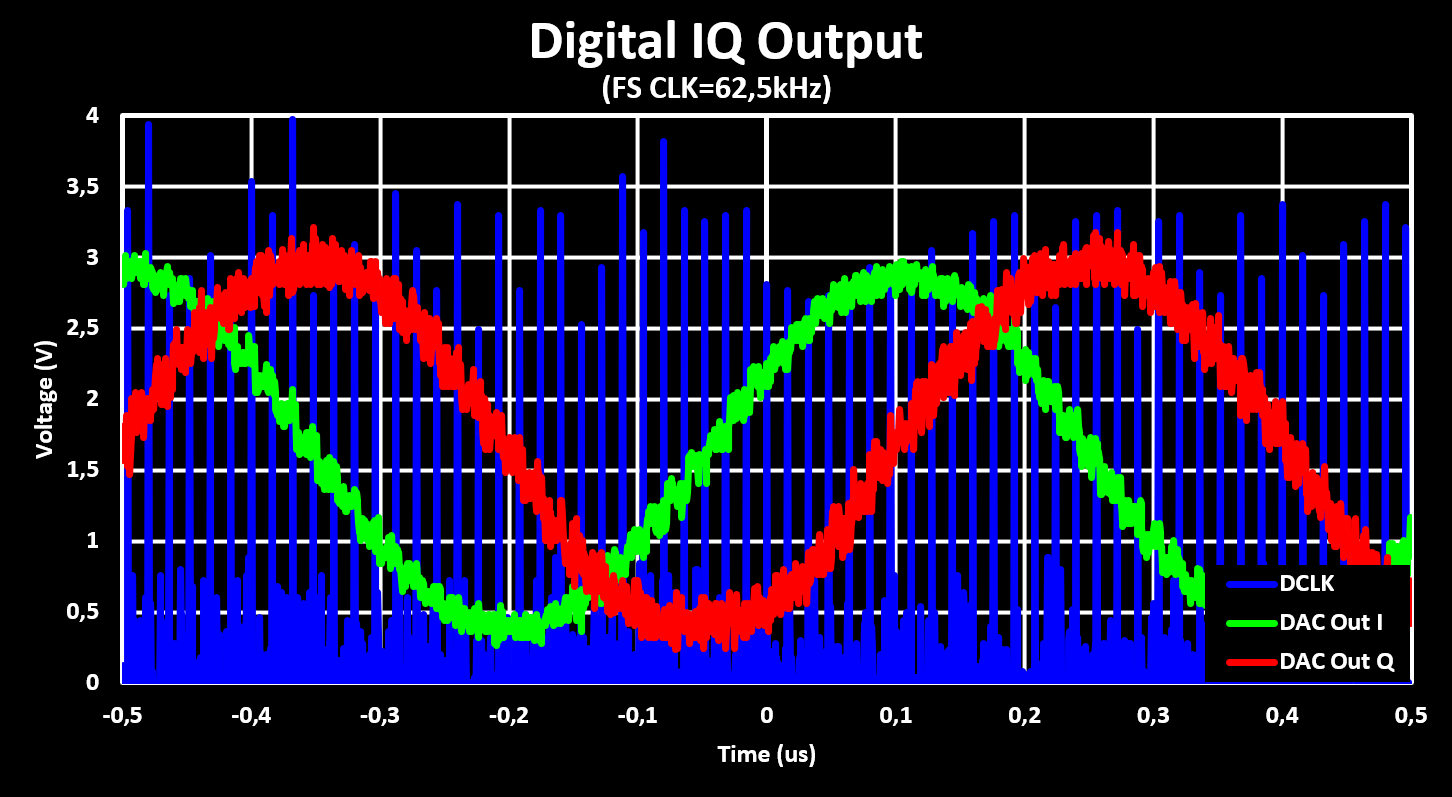
It is not very clear what each of these data options are, but it can be guessed from their name. The length, number of bits, of each data option is also unclear, from experiments it seems that most are 16-bits long, 32-bits for I/Q modes with 16-bits used for each I and Q data. Not all data options can be enabled at the same time, the maximum frame length is 72 bits, but is gets shorter with high datarate data e.g. for a system clock of 16 MHz and outputting I/Q data (32-bits), the maximum data rate is 500 ksps, which gets lower if more data is output at the same time.
To see how the dedicated digital interface works, to get the bit framing, the AX5043 was programmed to output the baseband I/Q data by setting register DSPMODECFG (0x320) to 0x03 and DSPMODESKIP1 (0x321) and DSPMODESKIP0 (0x322) registers to 0x7F and 0xFD respectively. With this, the following signals are output on the interface pins:
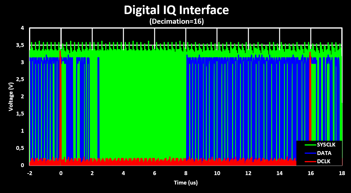
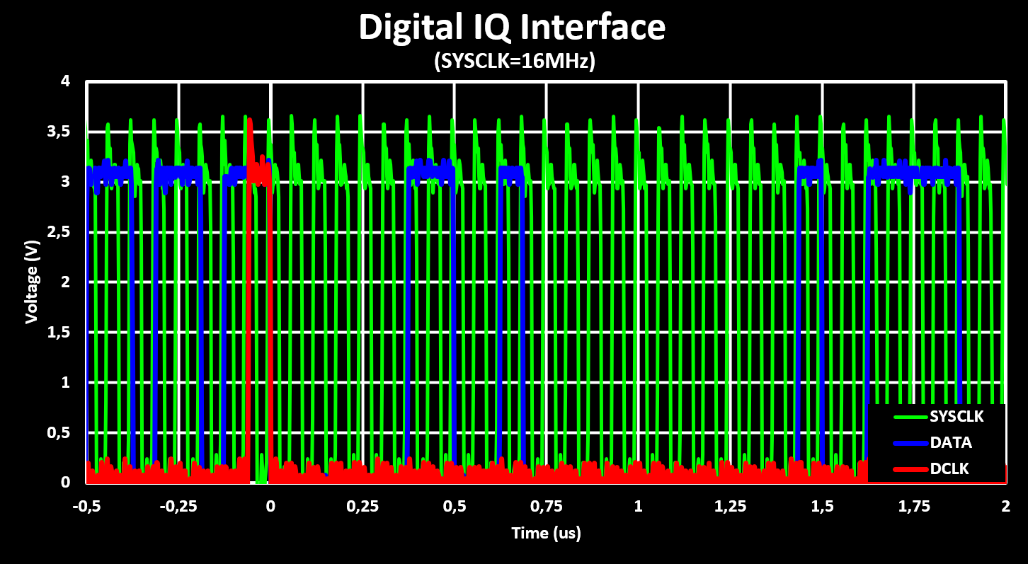
The first observation is that the bit clock, on SYSCLK pin, is output continuously and that the frame sync, on DCLK pin, is only one bit long. Also, there can be random data on the data line, on DATA pin, after the valid frame bits which in this case is after the first 32 bits. A close up of the initial part of one frame is shown in the figure bellow:
I found that the best way to interface with this digital interface is with a MCU that has a SAI peripheral, the framing of the digital interface is very similar to SAI TDM frame. This is my preferred way of reading the baseband I/Q signals from the AX5043, and was tested and used both on a STM32G473 and on the MIMXRT1060-EVKB board. Another way of interfacing with the digital interface is using a SPI peripheral that supports pulsed CS, or SPI TI mode, which was also tested with success on the STM32G473. The figure bellow shows the acquisition with the SAI peripheral of the STM32G473 and subsequent output of the data through two of its internal DACs.