The inspiration for this DAQ project came while working on some hardware, and firmware, debugging at home and realising that the only test equipment I had at hand was a multimeter. This sparked at first the idea of developing a simple USB oscilloscope with 2-4 Input Channels and 1-2 Output Channels using only a MCU with some external analog circuitry, basically a more advanced DSO138. After realising that this was not very feasible do to the integrated USB controllers of most MCUs being only USB-FS (12 Mbits/s) and also that a DAQ was more what I needed, the oscilloscope idea was abandoned, at least for now.
The first and simplest solution to this lack of equipment would be buying a DAQ but because I didn’t need it urgently and it looked like a fun new project I decided on developing my own. And if a couple of bucks could be saved on the way while also developing something more configurable even better. The first thing then was to set the minimum requirements. I looked up a few of the most popular and cheap commercial DAQs like the NI-DAQ USB 6009, the LabJack U3-HV and the Simultan USB-1608FS-Plus, which gave me an idea of what are the standard features and performances for a entry level USB DAQ, which I wanted to meet or exceed. Of course without the extensive software libraries and compatibility the commercial ones offer and which is a big part of their value.
Based on this research and on what features I wanted, the minimum requirements for the DAQ were established. It had to have at least 4 differential channels where each input could also be used as a single ended channel. The analog inputs needed to have different ranges, up to $ \pm 10V $, and sampling rates over 10 ksps. It should also have at least two analog outputs also ranging up to $ \pm 10V $ as well as fixed 3.3V and 5V outputs. The final requirement was having a couple of GPIOs that preferably could be used for digital communication protocols such as I2C, SPI and/or UART. Of course the whole DAQ has to operate from a single USB connections and no additional power source.
Currently the real features and characteristics of the DAQ are the following:
Two Analog Input Blocks with each:
- 4 differential, 8 single ended Inputs
- 12 bit ADC resolution
- Up to 62.5 KSPS sample rate, shared between channels
- Input range from $ \pm 12V $ down to $ \pm 16mV $
Two Analog Output Blocks with each:
- 5V 200mA and 3.3V 200mA power outputs
- Programmable current source from 100uA to 1.5mA
- 2 Analog Outputs with $ \pm 12V $ output range, 12 bit resolution and up to 1 MSPS
Digital IO Block with:
- 16 GPIOs with 5V level shift circuitry (max. 1 MHz)
- SPI, I2C and UART hardware decode interfaces
- 5V 200mA and 3.3V 100mA power outputs
Version History
Revision 1
Schematic: STM32G4_DAQ_Schematic_V1.pdf
Gerber: STM32G4_DAQ_Gerber_V1.zip
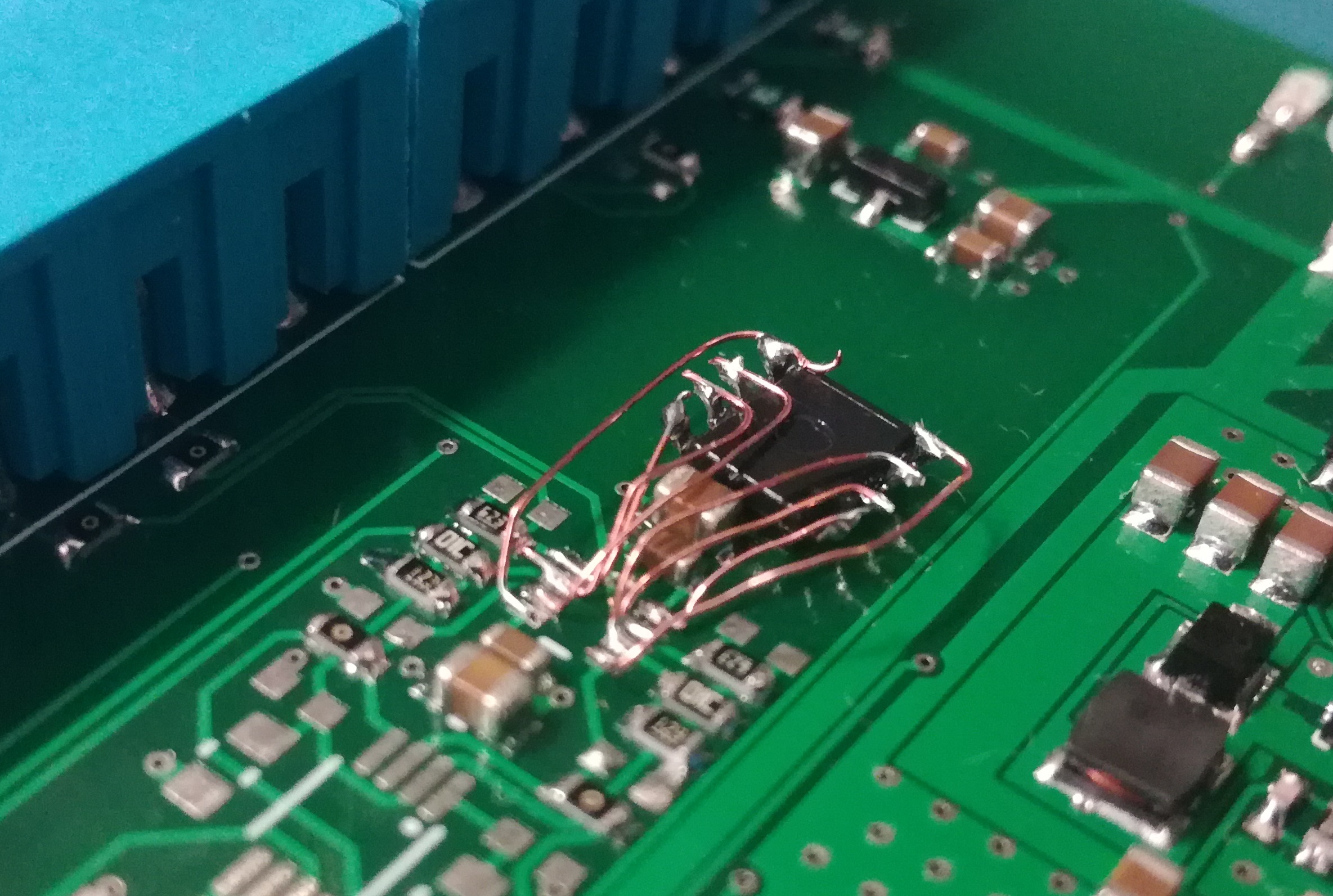
This is the first and current hardware version in development and testing. So far no major errors where detected but there is still a lot to be tested and validated. For now, the only mistake is the footprint used for the analog output amplifier, a SOT23-8, with only one IC that fits and meets the required characteristics, the OPA2991, which is not yet widely available. In a future version this footprint will be changed to a more common footprint like SOIC-8 or VSSOP-8. For now a OPA1678 (SOIC-8) OpAmp, one that was at hand, is bodge installed to test the Analog Output. This artistic installation can be seen on the figure bellow:
Overview
The design that I came up with is built around the STM32G4 MCU, a new MCU from STMicroelectronics developed for analog and mixed signals applications with an extensive list of analog peripherals like five 12-bit ADCs and seven 12-bit DACs. The analog input circuit is developed around the new ADA4254 from Analog Devices with a multiplexer connected to it to get the desired number of analog input channels. The different functional blocks are arranged according to the figure bellow:
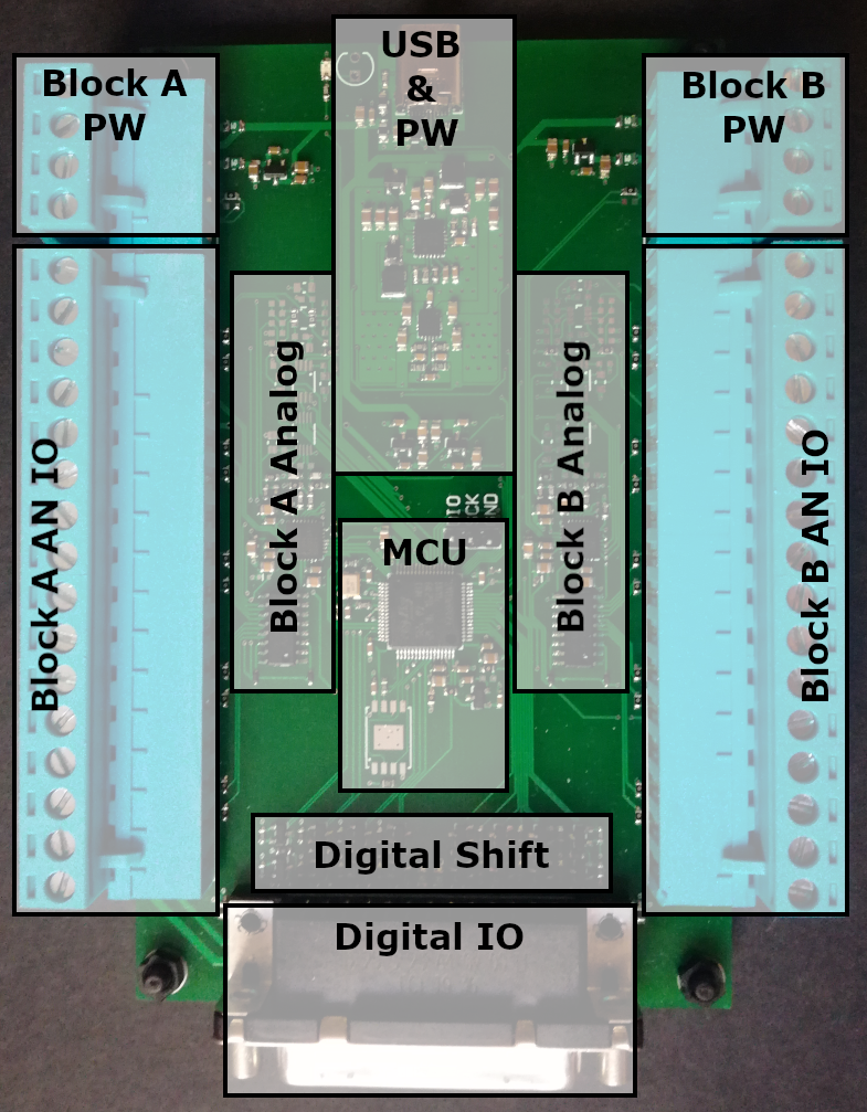
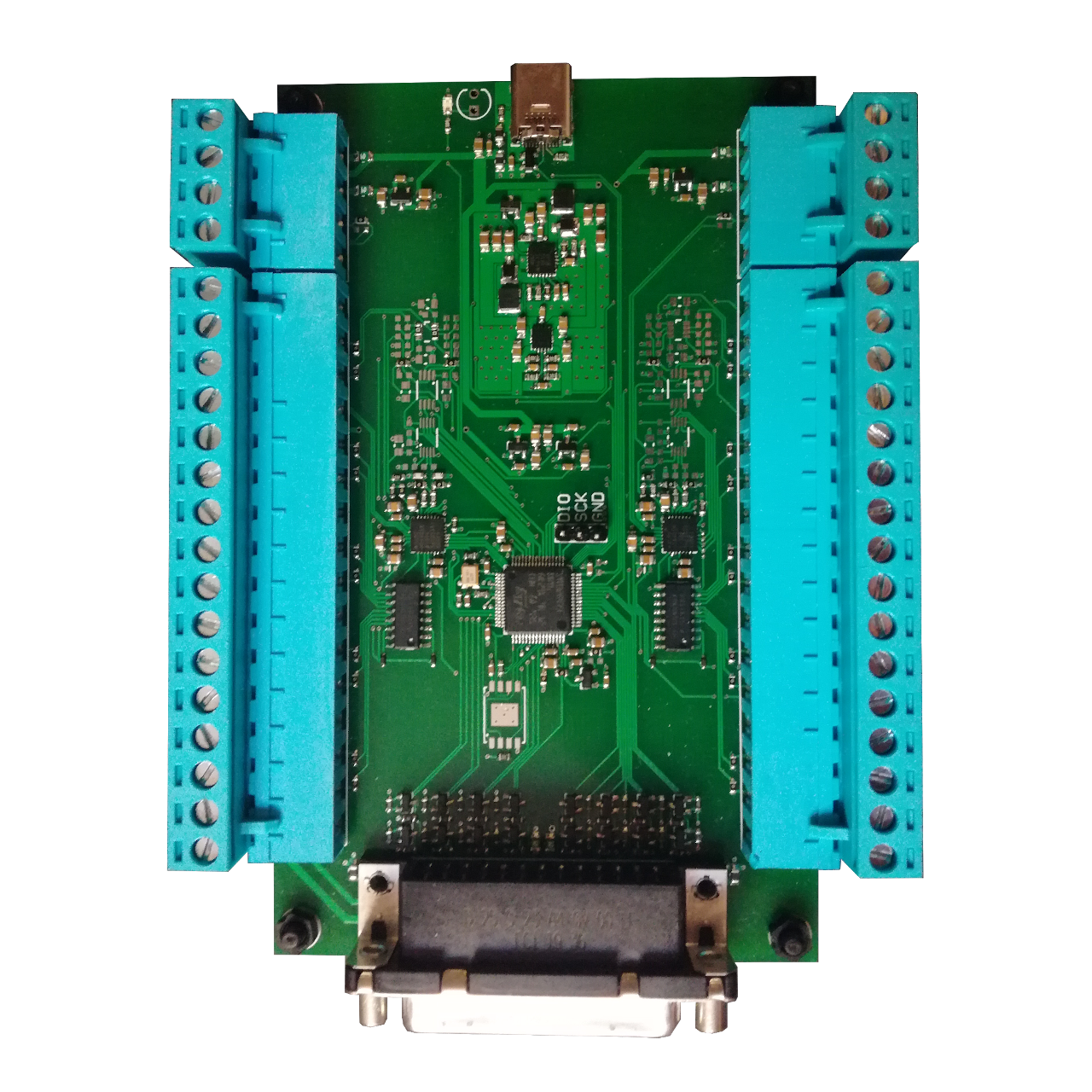
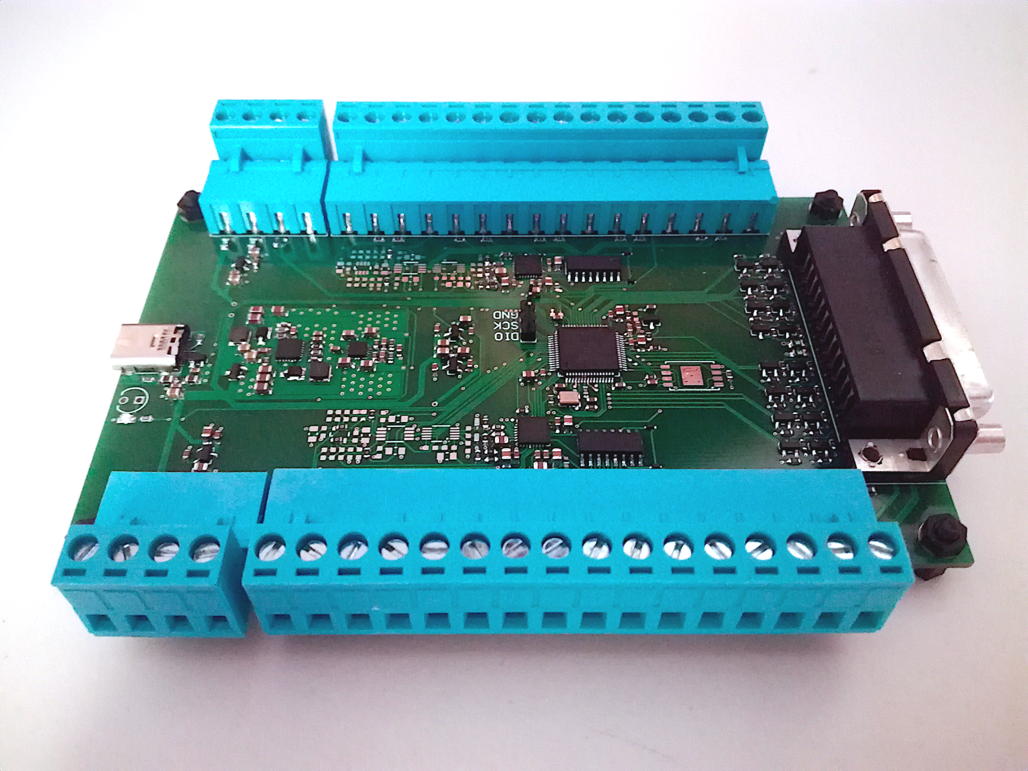
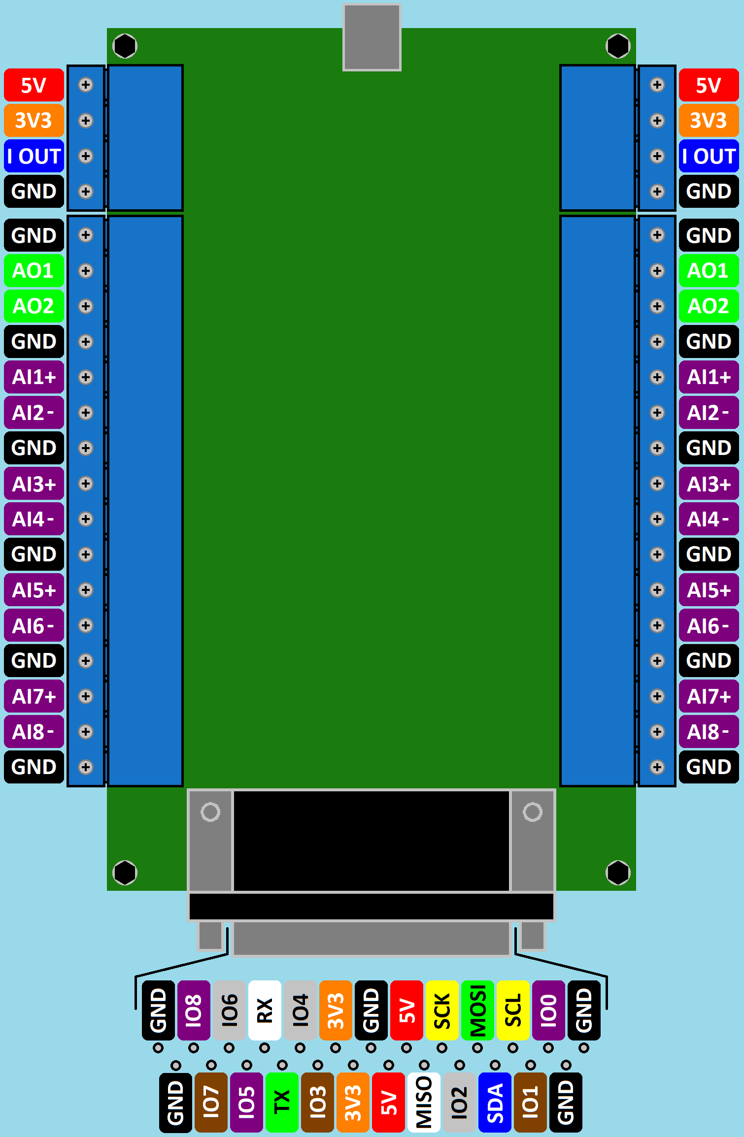
This figure shows that the analog interfaces are split into two blocks called Block A and Block B, one on each side of the PCB. Each of these blocks has its own output power domain on a 4 terminal connector as well as independent analog input and output circuitry on the 16 terminal connector. The connector used for the analog IO is a 5mm pitch plugable terminal block, commonly used by many DAQs, offering great flexibility and ease of use. For the Digital IO a 25 pin D-SUB (DB-25) connector is used, located at the bottom of the PCB. The simplified layout of all the connectors on the board and their respective pinouts is shown in the figure bellow:
Power Domain
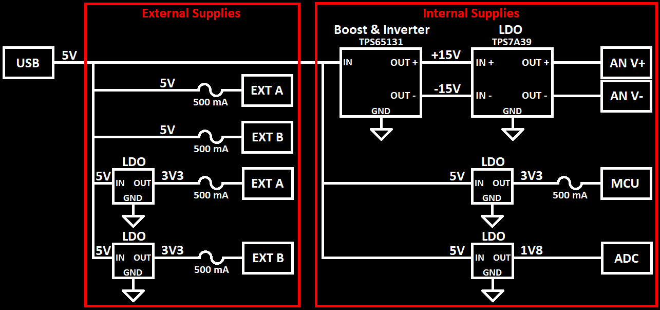
All the power rails used are derived from the USB VBUS. This simplifies the connection needed for the DAQ but also limits the combined power draw from all power rails to 2.5 Watts as most USB connections only allow for 500mA @ 5V, the basic power delivery specification for USB 1.0/2.0. This is not a problem for powering the DAQ as its consumption in normal operation is bellow 500mW but it limits what external circuits can be powered from the DAQ power outputs.
As seen in the overview section, each analog block has a power output block with 3.3V and 5V outputs that can be used to power external circuits. Each of these outputs has a 500mA protection fuse. The 5V output are powered directly from to the USB VBUS while the 3.3V outputs are each powered from an independent LDO, the TPS7A05, which is capable of delivering up to 200mA. The 3.3V output from the Digital IO shares the LDO used to power the internal ICs as well as the digital voltage shift circuitry. This limits the available current output of this output to about 100mA.
To generate the positive and negative rails for the analog circuits a combined Boost and Inverter switching converter is used, the TPS65130. This chip is set up to generate 15V on the positive rail and -15V on the negative rail, from the 5V input. Both these rails then pass trough an LDO for filtering/smoothing. The LDO chosen for this is a combined positive and negative rail LDO, the TPS7A39, which has a high PSRR of over 50 dB. This LDO is set up to output $ \pm 14V $. An additional LDO is installed to generate the 1.8V needed for an external ADC but this option is currently not used.
The power supply architecture is resumed in the block diagram bellow.
Analog Input
At the heart of each Analog Input Block is the ADA4254, a zero drift Programable Gain Instrumentation Amplifier. It provides programmable gains from 1/16 to 128 with input signal ranging up to $ \pm 28V $. It also does the output scaling so that a differential ADC can be connected to it directly. Besides that it also has a two channel input multiplexer as well as GPIOs that can control an external multiplexer and output the internal clock. It also has a programmable current source. All this made it the perfect choice for this project. In the beginning a more discrete implementation for the PGA and ADC input scaling was considered but that was abandoned because using the ADA4254 safes cost and circuit complexity.
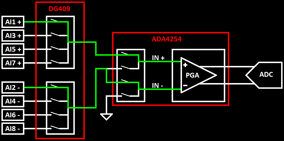
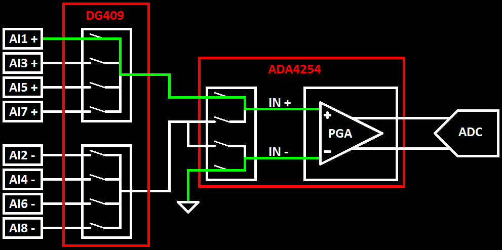
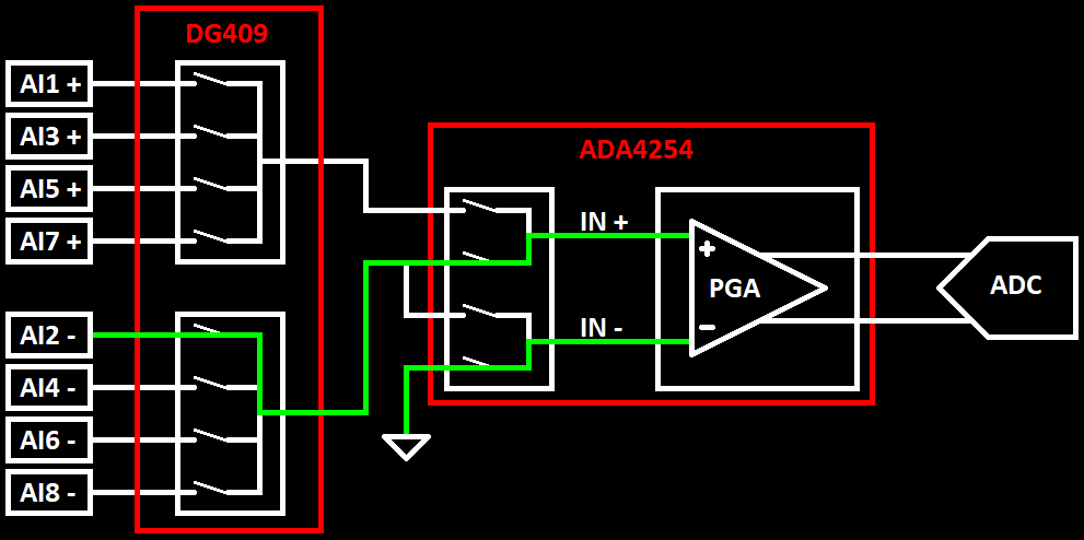
To get the desired number of input channels, a dual 4-Channel analog multiplexer is added, the DG409. This multiplexer is connected to and controlled by to the ADA4254. One of the 4-Channel Mux is used for the positive differential inputs while the other is used for the negative inputs. The internal 2-Channel Mux of the ADA4254 is used to either connect both inputs to the external Multiplexer, in differential mode, or connect only one of them and connecting the other to ground, in single ended mode. The block diagram of the Analog Input block and the connection logic for each mode is visible in the figures bellow:
As the ADA4254 already handles the output scaling and $ V_{OCM} $ shift, it is directly connected to a differential ADC with only a simple RC anti-aliasing filter in-between. The differential ADC can either be an external one or the STM32G4 internal one. The current version uses the STM32G4s internal 12 bit ADC with a $ V_{REF} $ of 2.048V also provided by the internal $ V_{REF} $ buffer of the STM32G4. The $ V_{OCM} $ of 1.024V is provided by a simple resistor divider network. This configuration provides the following input ranges and resolutions:
| Gain | Range | Resolution |
|---|---|---|
| 1/16 | $ \pm $ 32.768 V | 16 mV |
| 1/8 | $ \pm $ 16.384 V | 8 mV |
| 1/4 | $ \pm $ 8.192 V | 4 mV |
| 1/2 | $ \pm $ 4.096 V | 2 mV |
| 1 | $ \pm $ 2.048 V | 1 mV |
| 2 | $ \pm $ 1.024 V | 500 uV |
| 4 | $ \pm $ 512 mV | 250 uV |
| 8 | $ \pm $ 256 mV | 125 uV |
| 16 | $ \pm $ 128 mV | 62.50 uV |
| 32 | $ \pm $ 64 mV | 31.25 uV |
| 64 | $ \pm $ 32 mV | 15.63 uV |
| 128 | $ \pm $ 16 mV | 7.81 uV |
To note here that the actual input range is limited to bellow $ \pm 13V $. This because both the multiplexer and the amplifier inputs are limited to bellow their supply voltage. As both are powered from the $ \pm 14V $ power rails and, in case of the amplifier, also having protection diodes in series to its input supplies, the effective input range is a little over $ \pm 13V $.
Analog Output
As seen in the overview section, each analog block has two analog voltage outputs that can output up $ \pm 14V $. The PCB is designed to allow the use of the MCUs internal DAC or an external dual DAC. The output of the DAC is then amplified by an Operational Amplifier to the full analog voltage range of $ \pm 14V $. The circuit used for this is shown in the figure bellow and was copied from a Reference Design from TI.
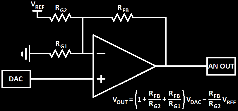
The current configuration uses the MCUs internal DACs with a $ V_{REF} $ of 2.048V provided by the internal $ V_{REF} $ buffer of the STM32G4. With this, the values of the resistors can be calculated by substituting the voltage values in the circuits equation for different states, starting with the negative full-scale output state, where $ V_{DAC} = 0V $ and $ V_{OUT} = -14V $:
$$ -14V = \left( 1 + {R_{FB} \over R_{G2}} + {R_{FB} \over R_{G1}} \right) (0V) - {R_{FB} \over R_{G2}} (2.048V) $$
$$ R_{FB} = {14 \over 2.048}R_{G2} $$
The other state used is the positive full-scale output, where $ V_{DAC} = V_{REF} = 2.048V $ and $ V_{OUT} = 14V $:
$$ 14V = \left( 1 + {R_{FB} \over R_{G2}} + {R_{FB} \over R_{G1}} \right) (2.048V) - {R_{FB} \over R_{G2}} (2.048V) $$
$$ R_{G1} = {R_{FB} \over \left( {14 \over 2.048} - 1 \right)} $$
The final step is to seed/choose the value of $ R_{G2} $. Here a value of 10K was chosen and with that the values for $ R_{FB} $ and for $ R_{G1} $ are calculated to being 68K and 12K respectively, rounded to the nearest E24 resistor values. This gives the final equation for $ V_{OUT} $ of:
$$ V_{OUT} = {202 \over 15} V_{DAC} - {68 \over 10}2.048 $$
As the MCUs internal DACs have a resolution of 12 bits, the $ V_{OUT} $ resolution is:
$$ \Delta V_{OUT} = {202 \over 15} \Delta V_{DAC} = {202 \over 15} * {2.048 \over 2^{12}} = 6.73 mV $$
It is important to note here that the OpAmp selected for this application has to have a very high slew rate so that it can follow the DAC output. As the internal DAC of the MCU can output a full range step, from 0 to 2.048V (4095), at a rate of 1 MSPS, the OpAmp has to have a slew rate greater then 28V/us to achieve a full -14V to 14V step at that sampling rate. The OpAmp slew rate is currently the limiting factor of the Analog Output of the DAQ as will be shown in the Results section.
Digital IO
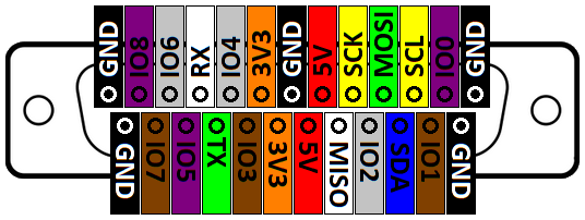
As seen in the Overview section, the DAQ has a Digital IO connector (D-SUB 25) that provides 16 digital Inputs and Outputs. Some of these are multiplexed with digital interfaces: 1 I2C, 1 SPI and 1 UART. The pinout of the Digital IO connector is shown in the figure bellow:
As the MCU operates at 3.3V and it was decided that the digital IO lines have to work at 5V, they have to be level shifted from/to 5V. This is done with a simple N-MOS bidirectional level shifter shown in the figure bellow:
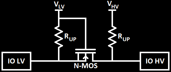
This circuit is very simple but has many drawbacks that were only realized during testing. In output mode, MCU as output, it is effectively a open-drain output where the drive capabilities are limited by the $ R_{UP} $ resistor value. In input mode, the same $ R_{UP} $ resistor is the input impedance. Also driving either side low results in a static current consumption which depends on $ R_{UP} $ and that can be calculated by the following equation:
$$ I_{LOW} = {V_{LV} \over R_{IP}} + {V_{HV} \over R_{IP}} $$
Finally, this resistor also limits the maximum frequency of the GPIOs, the higher the value the lower the maximum frequency is. It also depends on the N-MOS used, here the 2N7002, but this is harder to control. The effect of the $ R_{UP} $ resistor on the maximum GPIO frequency will be shown in the Results section.
The software of the DAQ is split into two parts, the DAQ firmware and the Driver/Support software on the PC. The firmware is written in C and uses the Low Level (LL) peripheral library provided by STM as well as the USB stack library also provided by STM. On the PC side, currently only a C# library to interface with the DAQ is in development as well as a visual interface using WPF. All the software is still in very early stages and under development. In the future a Python interface library is also planned.
The USB interface between the DAQ and the PC uses the CDC driver from STM which works in bulk transfer/endpoint mode. This mode enables the highest throughput. The CDC driver uses a Virtual COM class and is therefore easily detected and accessed on the PC through a serial COM connection. The communication is done in bytes and not in ASCII for increased performance and reduced overheads.
The full software is available on my Github:
Interface Protocol
To get the highest throughput on the USB interface, the control and communication protocol with the DAQ is done in raw byte packages. These packets consist of 4 fields as can be seen in the table bellow:
| Byte # | 0 | 1&2 | 3 -> N | N+1 & N+2 |
|---|---|---|---|---|
| Meaning: | Opcode | Length | Payload | CRC |
| Format: | u8 | u16 | N * u8 | u16 |
The Opcode section indicates what command or data is being transmitted, the significance of the payload field. The Length field indicates the length of the payload field, in bytes. The Payload field is a byte array of length equal to what is indicated in the Length field. The CRC field is used for packet validation but is currently not used, it is set to 0.
The currently implemented commands and data packets can be organized into two groups: The ones that are sent from the PC to the DAQ, generally only command packets, and the ones sent from the DAQ to the PC, generally only data packets. The Table bellow shows a resumed list of all available command packets, sent from the PC to the DAQ.
| ID | Opcode | Command | Payload |
|---|---|---|---|
| 0x01 | RESET | Reset the DAQ | None |
| 0x02 | CONNECT | Connect to the DAQ | None |
| 0x03 | DISCONNECT | Disconnect from the DAQ | None |
| 0x11 | SET CURRENT A | Set Current Output A | 2 bytes |
| 0x12 | SET CURRENT B | Set Current Output B | 2 bytes |
| 0x13 | SET ANALOG IN A | Set Analog In Block A | 2 bytes |
| 0x14 | SET ANALOG IN B | Set Analog In Block B | 2 bytes |
| 0x15 | SET ANALOG IN A CHANNEL | Set Analog In Block A Channel | 5 bytes |
| 0x16 | SET ANALOG IN B CHANNEL | Set Analog In Block B Channel | 5 bytes |
| 0x17 | SET ANALOG OUT A CHANNEL | Set Analog Out Block A Channel | 6+N bytes |
| 0x18 | SET ANALOG OUT B CHANNEL | Set Analog Out Block B Channel | 6+N bytes |
Table bellow shows a resumed list of all available data packets and there respective Opcodes, sent from the DAQ to the PC.
| ID | Opcode | Command | Payload |
|---|---|---|---|
| 0x81 | ANALOG IN A | Analog In A Data/ADC Samples | 1+N bytes |
| 0x82 | ANALOG IN B | Analog In B Data/ADC Samples | 1+N bytes |
Bellow is a more in-depth explanation of each Command and Data Packet and there respective payload.
RESET (0x01)
Resets the DAQ.
Payload: None
CONNECT (0x02)
Connect to the DAQ. Data communication is only possible after this command. This command is necessary for the DAQ to know that the PC Software is ready for Data, that it is running.
Payload: None
DISCONNECT (0x03)
Disconnect from the DAQ. The DAQ turns Analog Input sampling off and clears all Analog Input sample buffers.
Payload: None
SET CURRENT (0x11/0x12)
Set the current outputs of the DAQ. Current outputs are from the ADA4254 IC.
Payload:
- Source (u8): Selects the voltage source for the current source:
- 0x00: None
- 0x01: Low Voltage
- 0x02: High Voltage
- Value (u8): The current output value, in 100uA steps:
- 0x00: 0uA
- 0x01: 100uA
- …
- 0x0F: 1500uA
SET ANALOG IN (0x13/0x14)
Set Analog In Block configurations. These are shared settings between all input channels of an Analog Input Block.
Payload:
- Rate (u8): Sets the Analog In sample rate, in 1/2 steps:
- 0x00: 250 ksps (Reserved, do not use)
- 0x01: 125 ksps (Reserved, do not use)
- 0x02: 62.5 ksps
- 0x03: 31.25 ksps
- …
- 0x0B: 122 sps
- Scale (u8): Sets the ADA4254 output amplifier voltage scaling
- 0x00: 1 V/V
- 0x01: 1.25 V/V
- 0x02: 1.375 V/V
SET ANALOG IN CHANNEL (0x15/0x16)
Set Analog In Channel configurations. The independent settings for each Analog Input Channel.
Payload:
- Channel (u8): The Analog Input Channel number, of this analog block.
- Mode (u8): The Analog Input mode for this Channel
- 0x00: Off
- 0x01: Differential Ended Mode
- 0x02: Single Ended Mode
- Division (u8): Sets the sampling rate subdivision of this channel. NOT USED!
- Resolution (u8): Sets the Analog Input ADC resolution, in 1-bit steps. NOT USED!
- 0x00: 8-Bits
- 0x01: 9-Bits
- …
- 0x08: 16-Bits
- Gain (u8): Sets the Analog Input range/gain, in x2 Gain, 1/2 range steps.
- 0x00: 1/16 Gain, $ \pm 32V $ range (Reserved, do not use)
- 0x01: 1/8 Gain, $ \pm 16V $ range
- …
- 0x0B: 128 Gain, $ \pm 16mV $ range
SET ANALOG OUT CHANNEL (0x17/0x18)
Set Analog Out Channel configurations. The independent settings for each Analog Output Channel.
Payload:
- Channel (u8): The Analog Output Channel number, of this Analog Block.
- Frequency (u24): The DAC sample frequency to use in Hz. Maximum recommended is 1Msps, absolute maximum is 5Msps.
- Buffer Length (u16): Number of samples (u16) of the Analog Output buffer. Maximum buffer length is 128.
- Buffer (u16): Array of samples for the Analog Output buffer of Length Buffer Length.
ANALOG IN DATA (0x81/0x82)
Analog Input Data packet sent to the PC from the DAQ. This is a collection of all samples of all channels of an Analog Input Block. The samples are in raw ADC counts.
Payload:
- Channel (u8): The Analog Input Channel number, of this analog block.
- Samples (u16): Array of samples, ADC Counts, from the Analog Input Channel specified in Channel with a length of $ {Length - 1} \over 2 $.
PC Software
The PC Acquisition Software is currently capable of controlling both the Analog Block A and B. On the analog Input side, all the main functionalities like sampler rate, Single/Differential Mode and Range/Gain are implemented and working. The PC driver gets the data from the DAQ in realtime and the Acquisition Software updates the Window with them every 100ms. In the beginning the Graphing library used was LiveCharts, which looks great but is very slow in drawing, at least the free version. It was later changed for the open source ScottPlot which is simpler and much much faster. With LiveChart I was not able to get the Chart to update reliably every 1s, with ScottPlot even plotting a new Chart every 100ms is easy (drawing 2 sets/plots of 512 points each).
The PC Software can also control the analog outputs of the Analog Block A and Block B. It can, for now, generate DC outputs, Sine waves, Square waves and Ramps with frequencies from 1 Hz to 100 kHz with configurable amplitudes and offsets. For all these, the number samples used to generate the signal varies with the signal frequency, at the highest signal frequency, 100 kHz, 20 samples are used and this is increased to a maximum of 100 samples for decreasing frequencies, for 10 kHz and lower.
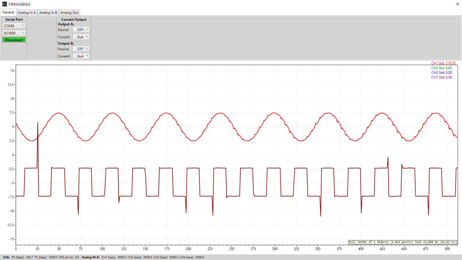
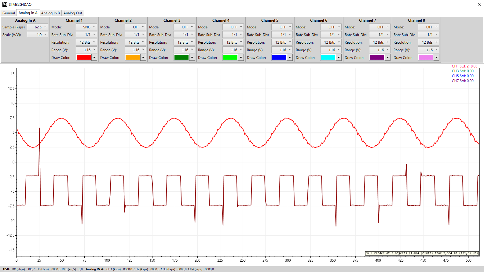
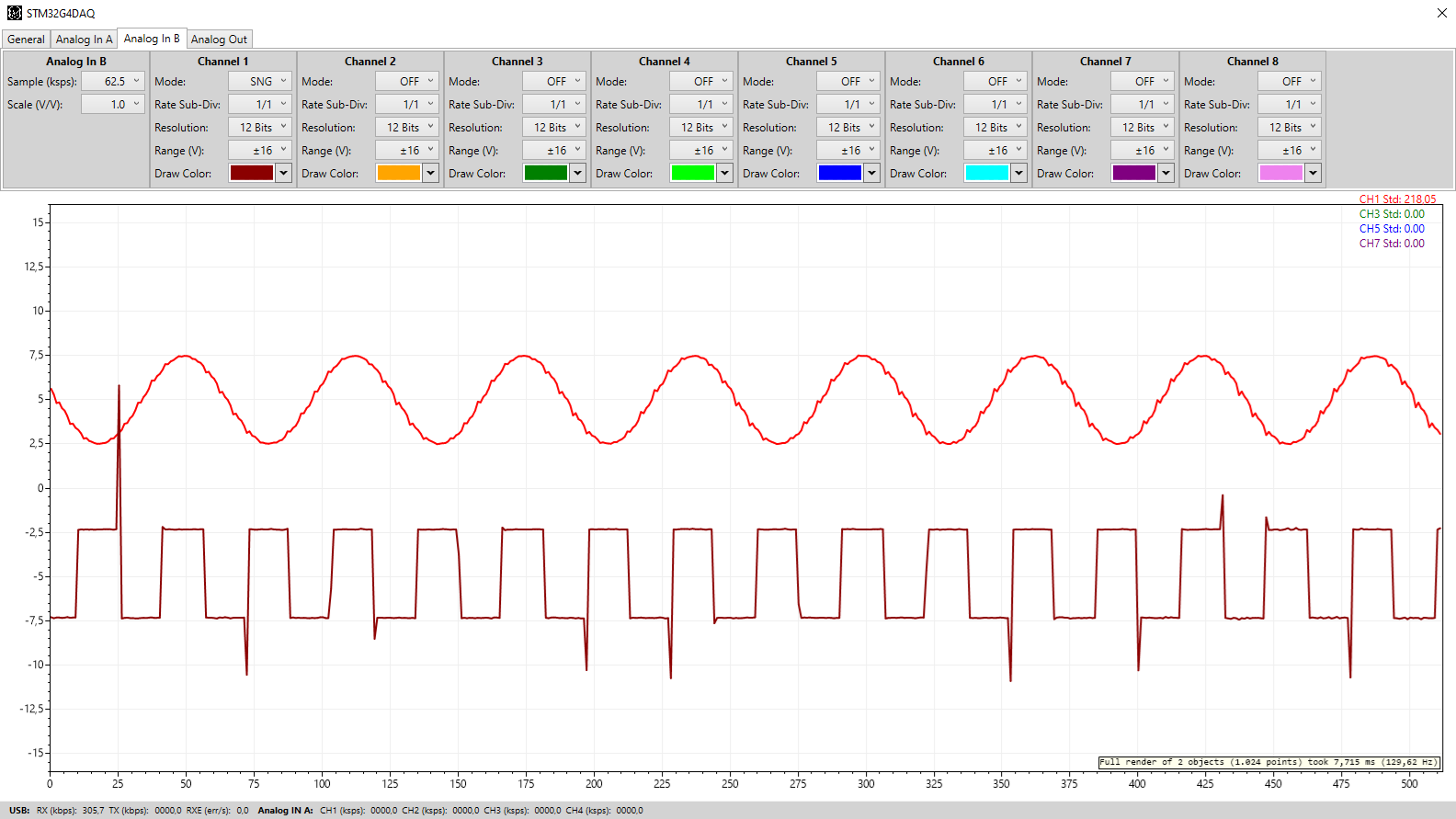
Bellow is a Figure showing all the control Menus of the PC Acquisition Software, the first tab is the General Menu where the COM port is selected and connection is established (baud rate value is irrelevant). The second tab is the analog input control for block A, the third for block B and the forth the analog output control. On the bottom is a bar indicating the current USB RX speed, the other values are not updated/used. The shown signals are generated by the analog outputs of channel 1 and 2, and are acquired by the analog input channel 1 from block A in red and channel 1 of block B in dark red, with the settings visible in the tabs.
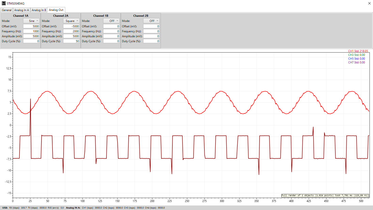
These figures show the generation of a sine wave on the Analog Output 1 and a Square wave on Analog Output 2. Both are generated with 100 sample points as the signal frequency is below 10 kHz. Besides sine waves and square waves, the two signals shown in the above figure, the PC Software can also generate DC signals as well as Ramp signals with programmable slope lengths. The center of the ramp, highest point, is controlled by the duty cycle control. Using a duty cycle of 50% results in a a triangular wave, using a duty cycle over 50% results in a longer rising slope and a duty cycle bellow 50% in a longer falling slope. An example of a generated ramp signal, and another square wave, can be seen in the figure bellow, including the configuration used for the Analog Outputs.
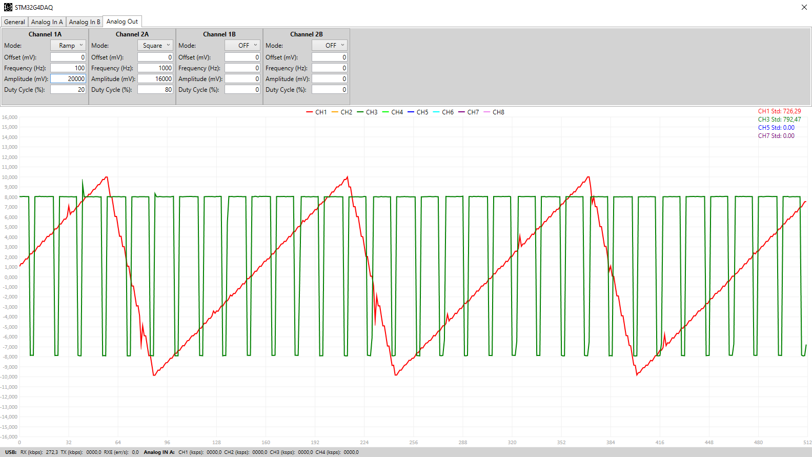
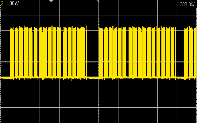
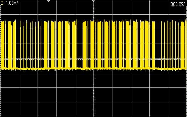
The output signal from the figure above can also be seen in the Analog Output section, in the last figure, captured by an oscilloscope. In the acquired signals by the DAQ and displayed on the PC Software there are some very pronounced spikes, the exact origin of these is not yet clear. By comparing both the PC Acquisition Signal and the oscilloscope signals it is possible to conclude that the spikes are not from the Analog Output as they don’t appear on the oscilloscope measurements. Therefore they must be an artefact from the Analog Input, either from the analog input circuitry or from the ADC sampling and the digital chain.
Power Domain
The analog power rail LDO (TPS7A39) outputs have a voltage noise/ripple of 6 mV RMS on the positive rail and 3 mV RMS on the negative rail.
USB Connection
As seen in the Software section, the USB connection is used in bulk transfer mode. This mode has a theoretical limit of 19 micro-frames every 1ms with each 64 bytes of payload, resulting in a maximum throughput of 1.216 MBytes/s, for USB-FS. In practice, using the STM32G4 and the USB CDC library from STM, a maximum throughput of ~750 kBytes/s was achieved, when no other processing is done on the MCU besides the USB stack and the USB Library is feed an array of 1024 bytes. This lower performance from the theoretical limit is due to the USB library needing to copy the passed array to the USB output buffer which takes time. This can be seen in the figure bellow where the USB D+ line is monitored:
The micro-frames are well visible and it can be seen that after every 16 micro-frames a interval with no transmission appears. This is when the USB Library copies a new 1024 byte array to the USB TX Buffer. Increasing or decreasing this array length doesn’t affect the throughput because with a larger array the coping takes more time less frequently and with decreased array lengths the coping is faster but more frequent. This limitation on the buffer copy can probably be reduced by modifying the USB CDC Library provided by STM or writing a new one.
In normal operation the throughput decreases further as the MCU is busy with other operations and the micro-frame processing sometimes can take longer and the array passed to the USB Library has to be built first. For the DAQ, the array passed to the USB Library is a temporary array built from coping data from the ADC read buffers. This means that for each transfer call two array copies occur. The effect of this two factors can be seen in the figure bellow where the USB D+ line is again monitored:
The figure shows both that the timing of each micro-frame is less consistent and the interval between subsequent transmissions is longer. This example uses again a 1024 byte array but this time copied from the ADC buffer which means that two 1024 byte copies are done for each transfer. Both these factors together decrease the USB throughput to a maximum of around 450 kBytes/s, this is still enough for the DAQ.
Analog Input
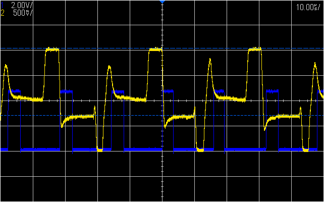
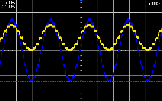
To achieve the zero drift, the amplifier uses a technique called chopping to remove DC drifts and offsets. This technique has the side effect of residual ripple on the output from the chopping and therefore, for best performance, the ADC sampling has to be synchronized with the chopping clock. The chopping frequency of the amplifier is 125 kHz, this clock is output and used by the MCU to synchronize the ADC. This means that the maximum sample rate of the ADC is 125 ksps. This output ripple can be seen in the figure bellow, note that the real ripple is the difference between the two differential outputs:
The real usable sample rate is further lowered by the fact that for each analog block all the inputs are multiplexed and share the same amplifier and ADC. Therefore, between each acquisition the gain of the amplifier has to be changed and the multiplexer input switched. It was decided that both the gain/range and the input mode can be programmed independently for each input channel.
The ADA4254 controls the gain/range of the analog input, which analog channel is being sampled by controlling the external multiplexer and the input mode, differential or single ended, with the internal multiplexer. The control of the gain of the amplifier as well as the control of the external multiplexer is handled by the same register, GAIN_MUX (0x00) register. The control of the internal multiplexer is handled by the INPUT_MUX (0x06) register. This means that after each acquisition, each channel switch, two registers have to be programmed.
The control of the ADA4254 is done with an SPI interface using 16 bit words where the first 8 bits are the register address and the second 8 bits the register data to write. At the maximum SPI clock the amplifier can handle, 5 MHz, each of this transactions take 3.2 us, so each channel switch take close to 10us with the CS timing included. This limits the maximum sampling rate to 62.5 ksps, the highest even division of 125 ksps that leaves enough time for ADC sampling and channel switching.
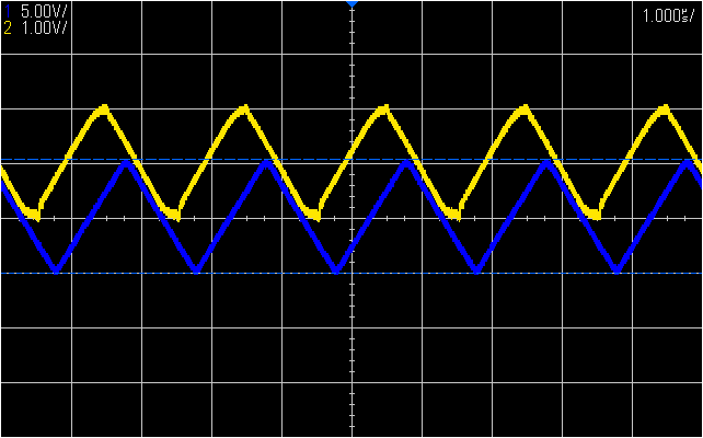
The figures bellow show the timing of a two channel acquisition in single ended mode at a sample rate of 15.625 ksps, with the input ranges set to $ \pm 1V $, $ \pm 4V $ and $ \pm 16V $ where one channel is connected to 0.9V, 3.9V and 12V respectively and the other channel is connected to -0.9V, -3.9V and -12V respectively. In blue the ADC interrupt handler timing is shown, triggered righter after a completed ADC conversion, in yellow is the SPI CS line to the ADA4254 and in red is the analog output of the amplifier, the ADC input.
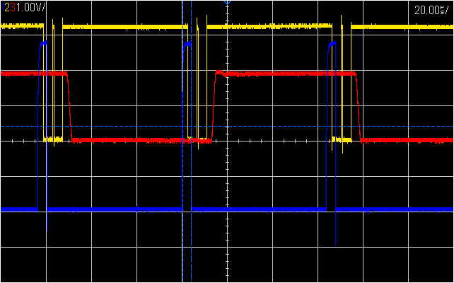
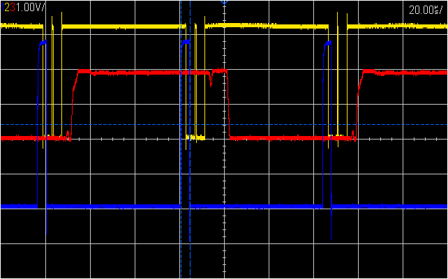
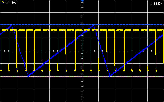
These figures show that the reprogramming of the ADA4254 takes the 10us mentioned before and also shows the settling time of the amplifier output for a full range step between channels when switching both the external and internal multiplexers. For the lower ranges, higher gains, the settling time is fast enough for use at the maximum sampling rate of 62.5 ksps. At the highest range, $ \pm 16V $, this is no longer true as it takes over 20us from register programing to a stable output. This is better shown in the figure bellow, sample rate of 62.5 ksps and $ \pm 16V $ range, where one channel was connected to GND and the other to 5V DC. In blue is again the ADC interrupt handler, the ADC conversion is done right before the rising edge, and this time in yellow is the ADA4254 output.
This figure clearly shows that the settling time of the ADA4254 output is to long, it is still settling when the ADC is sampling the signal, right before the rising edge of the blue signal. This means that when using more then one channel at the highest range, $ \pm 16V $, the maximum usable sampling rate is 31.25 ksps. On the next lower range, $ \pm 8V $, this is no longer a problem and it can be used with the highest sampling rate.
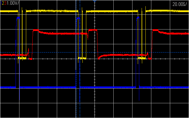
Also, at the highest range, $ \pm 16V $, the usable input voltage is lower then the range, at around $ \pm 13V $. Due to this, the output of the ADA5254 also doesn’t fill the full range and the switching of the internal and external multiplexer are visible. The internal multiplexer switch can be seen, on the output, as a step to 0V and is followed by the switch of the external mux, step to ~2V. Both of these switches have very visible over/under shoots. The internal mux is switched first as it was observed that it is slower then the external mux.
Noise
A noise performance analysis was performed by calculating the standard deviation of the ADC output in the PC software. The test was performed in differential mode and with two different test scenarios. The first is the best case scenario, only one channel is in use. The standard deviation was measured with the differential inputs shorted. For the highest range, lowest gain setting, the standard deviation is bellow 1 count. This increases to 2 counts when using the lowest range, highest gain. No difference was observed when changing the sample rate.
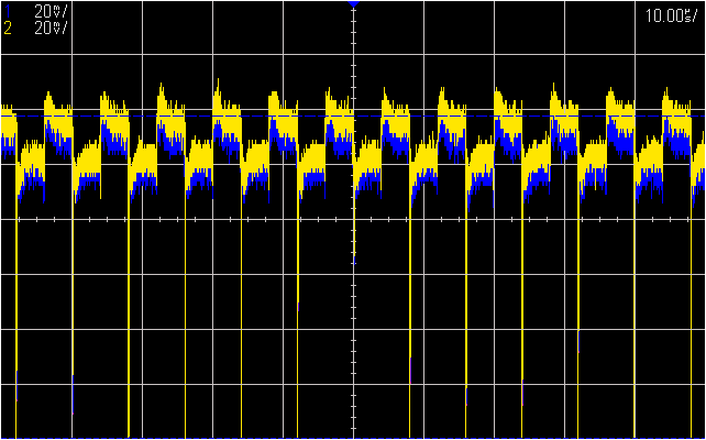
The second scenario is a worst case scenario, where two adjacent channels are used, Channel 1 and Channel 3. Channel 3 is left with the inputs shorted and on Channel 1 a random noise that fills the full scale is injected. This test was performed on the lowest range, highest gain setting, and the highest sample rate. The result of this test can be seen in the figure bellow, screenshot of the PC acquisition software.

The figure shows that the the standard deviation of Channel 3, in green, is bellow 3 counts even with the full scale noise on Channel 1, in red. Overall, in differential mode, the noise/standard deviation is always bellow 4 counts in all tested scenarios, for all channels, ranges and sampling rates. This is a good result and means that the DAQ has, in the worst case, 10-bits of effective resolution and virtually no crosstalk between channels.
Analog Output
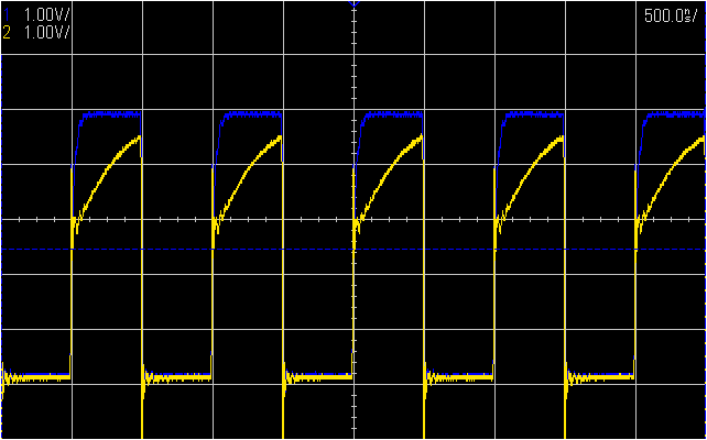
The internal DAC of the MCU can output up to 1 MSPS, limited by its settling time when stepping from the lowest count (0) to the highest (4095) which is around 1us. But in the current version the limiting factor is not the settling time of the DAC but the slew rate of the OpAmp used to boost the output voltage. Currently the OpAmp used is the OPA1678 with a slew rate of 9V/us. The figure bellow shows the test case where the DAC outputs full range steps at the 1 MSPS rate, the DAC output is shown in yellow and the OpAmp output in blue.
It can be seen that the DAC reaches, barely, the maximum output range of 0-2.048V but the OpAmp is not able to follow this, having a reduced output range of $ \pm 5V $ instead of the $ \pm 14V $. This is due to the slew rate of the OpAmp being only ~9V/us which is bellow the required slew rate of 28V/us. The OpAmp that was planned to be used is the OPA2991 that has a higher slew rate of 21 V/us, this is still bellow the required slew rate but is closer. This OpAmp will be tested soon.
This limitation is however not very relevant because to output a signal, besides a square wave, more then one sample is needed per period, reducing the step sizes and therefore the required slew rate. For example, to output a sine wave at least 12 samples should be used and with that, even when using the full range, neither the DAC nor the OpAmp has any problems. This example is shown in the figure bellow, the DAC output is displayed in yellow and the analog output, after the amplifier, in blue.
The Analog Outputs have independent control of all parameters including frequency as each DAC is triggered by a separate timer and has a separate circular sample buffer. This circular sample buffer is connected to the DAC through a DMA which sets the new DAC value at each timer trigger event. To increase the performance further the DAC buffer is located in the SRAM2 region, a separate and smaller region from the main SRAM. Both SRAM sections can be accessed simultaneously reducing MCU and DMA SRAM concurrent access wait states. The only time concurrent access conflicts occur is when the DAC buffer is set/changed, which is also the only time the MCU has to do processing for the Analog Output at all.
By using sample buffers and not local, in the DAQ, signal generation, the Analog Output can output any arbitrary waveforms that is programmed by the PC Software. The figure bellow shows the example of a Ramp signal output on Analog Output 1, in blue, and a square wave on Analog Output 2, in yellow.
This shows that the Analog Outputs are independently controlled, including the frequency. On the falling slope of the Ramp signal, in blue, the DAC samples/steps are visible.
Digital IO
As seen in the Hardware description section, the IO speed is limited by the $ R_{UP} $ resistor as well as the NMOS used, the 2N7002. This dependency on the $ R_{UP} $ resistor is shown in the figure bellow, where a $ R_{UP} $ resistor value of 1K, in blue, is compared to a $ R_{UP} $ value of 10K, in yellow, with the MCU generating a 1 MHz clock signal:
It is clearly visible that at 1MHz a $ R_{UP} $ value of 1K is needed, even when driving a high impedance load like the oscilloscope input (1 MOhm || 11pF). The limitation is the same when using the pin as input. This limitation is even more visible with a 5 MHz clock as shown in the figure bellow where, again a $ R_{UP} $ resistor value of 1K, in blue, is compared to a $ R_{UP} $ resistor value of 10K, in yellow.
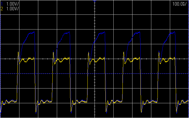
This shows that for signals over 1MHz a $ R_{UP} $ value lower then 1K has to be used. This comes, as seen in the hardware section, with the drawback of higher static current consumption in the low state and lower input impedance when being used as an input. All considered, the $ R_{UP} $ value chosen is 1K, which means that signals up to 1MHz can be output/input. This is considered a sufficiently high frequency as both the UART and I2C interfaces normally operate below 1 MHz and limiting the SPI interface to 1 MHz is also acceptable. Lowering the $ R_{UP} $ resistors further is not recommended as the static current consumption already is 8.3mA per pin, of which 3.3 mA has to be sinked by the MCU. This is not bad when only one pin is in the low state as the MCU can sink/source up to 20mA per pin but, when all 16 are in the low state, the combined current is over 52.8mA which is a little over half what the MCU can output (100mA) on all pins combined.
Using a $ R_{UP} $ value of 1K also means that the digital IO interface can drive outputs with a impedance higher then 10K and has an input impedance of 1K. These are not very good values and it has to be seen if they can be improved by using a different NMOS. Using different values for the High and Low side $ R_{UP} $ resistor was tested but the results show that the performance is limited by the higher of those values. In future hardware versions a different level shift circuitry will probably be used to improve performance.