Important Notice
The full Sub-GHz transceiver (the AX series) range of products from OnSemi have been discontinued, with end-of-life scheduled for december of 2022: Official Notice
This includes the transceiver used here, the AX5043, and all others from the same family, the AX5243 and the new AX5045 as well as the SoC (MCU+RF) versions of them, the AX8052F143 and the new AXM0F343.
While working on the TT&C of the first Portuguese Cubesat, ISTSat-1, I started to wonder what would be the simplest and cheapest way to receive and send data to this Cubesat. The TT&C uses UHF on the Uplink (436.45 MHz) and VHF (145.895 MHz) on the Downlink. The primary modulation and demodulation is AFSK, this to be compatible with HAM Radio stations. Other modulations used are G3RUH, a FSK modulation scheme also used by HAM Radios, (G)MSK, BPSK and QPSK. It also has a Morse Beacon on the VHF link.
Knowing this, the module needed to be able to handle AFSK Modulation in both VHF and UHF at a minimum, and at best all other modulations as well. Now this can be achieved with an SDR and GNURadio, using the cheap and ubiquitous RTL.SDR. For this a Linux PC with GNU Radio installed is needed. Also, the RTL.SDR is only a receiver, to have transmission as well a more expensive SDR is required, like a ADALM-Pluto or LimeSDR. Because of this, and because I wanted a simpler way and preferably not more expensive, I went a different route. The solution was using a Sub-GHz transceiver and a MCU to control it and decode the frames. Communicating with the PC is done over USB using Virtual COM.
Now finding a Sub-GHz transceivers is very easy, all of the major Semiconductor manufacturers have one kind or another. The difficult part was finding one that was able to use AFSK. This because it’s a double modulation and not very commonly used outside of HAM Radios. I only found one such transceiver, the AX5043 from OnSemi. As a bonus, this transceiver also supports many other modulations. From my findings it is actually the most versatile Sub-GHz transceivers out there.
Currently this module can modulate and demodulate AFSK, (G)FSK, (G)MSK and BPSK, both in UHF and VHF, with HDLC/AX.25 Framing, as well as Morse decoding using the RSSI. As special bonus feature of this transceiver, it can also receive and transmit FM audio signals and also receive AM audio signals.
Version History
Revision 3
Schematic: VUHF_Radio_Schematic_R3.pdf
Gerber: VUHF_Radio_Gerber_R3.zip
Assembly: VUHF_Radio_Assembly_R3.pdf
This version fixes all the hardware problem discovered in Revision 2, namely the power distribution and analog output filter and amplifier. The RF performance is the same as Revision 2, the new S11 values can be downloaded from the Matching Network section. Besides that the PCB color was changed to blue, which looks much better as can be seen in the figure below:
There are some small hardware mistakes in this version to:
-
In the analog input circuit, the differential amplifier has AC coupled inputs and therefore needs to have an AC coupling capacitor in the feedback loop instead of a direct connect to ground, this was missed in this version.
-
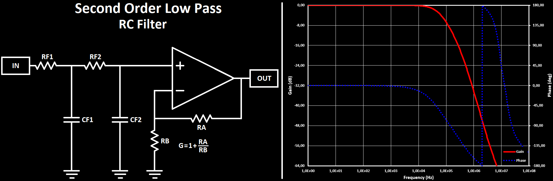
In the analog output circuit, the filter design used is not practical for this use case and has to be redesigned, probably to a 2 stage RC filter that was already tested.
Revision 2
Schematic: VUHF_Radio_Schematic_R2.pdf
Gerber: VUHF_Radio_Gerber_R2.zip
This version has some design errors that needed to be fixed with a new version:
-
The connections of the current sense amplifiers are wrong, the positive and negative inputs are switched up. I connected the input side of the sense resistor to the negative input of the amplifier instead of to the positive input…
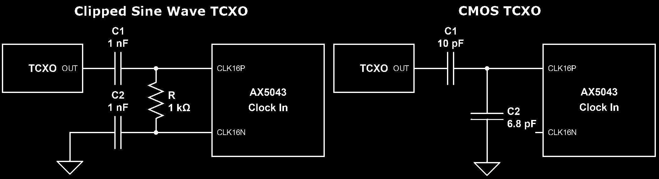
-
The TCXO interface circuit to the Radios is wrong, I used the schematic for a Clipped Sine Wave TCXO but the TCXO I have is a CMOS one. This is also the more common and therefore more easily available version. Below is visible the circuit needed for each one:
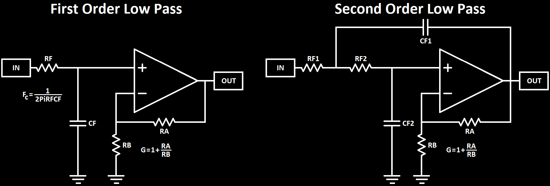
- Also the pinout of the single output Op-Amp is wrong, which is connected to the DAC output of the AX5043. I will also use this opportunity to change the filter architecture for the DAC output to a second order low pass one, from a first order. This change in circuit is in the Figure below:
Revision 1
Schematic: VUHF_Radio_Schematic_R1.pdf
Gerber: VUHF_Radio_Gerber_R1.zip
This version never got to test as it took over 2 months to ship and while waiting for it I found some errors and ordered the second version which arrived before the first one.
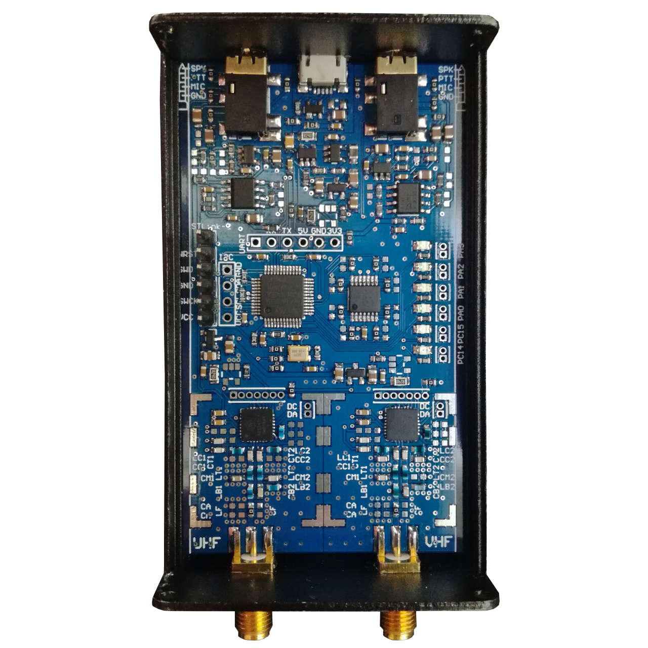
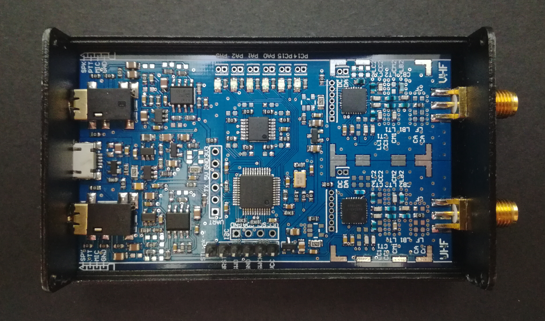
Overview
The PCB dimensions where chosen so that the module can fit inside a cheap and small aluminium enclosure, 80x50x20mm, widely found on eBay and AliExpress. For this enclosure the PCB has to be 48mm wide to fit snugly inside the support rails and can have a maximum length of 80mm. For this module the PCB length is 78mm to give space for the flange of the SMA connector.
I’m currently on the third Hardware version. The different functional blocks are arranged according to the figure below.
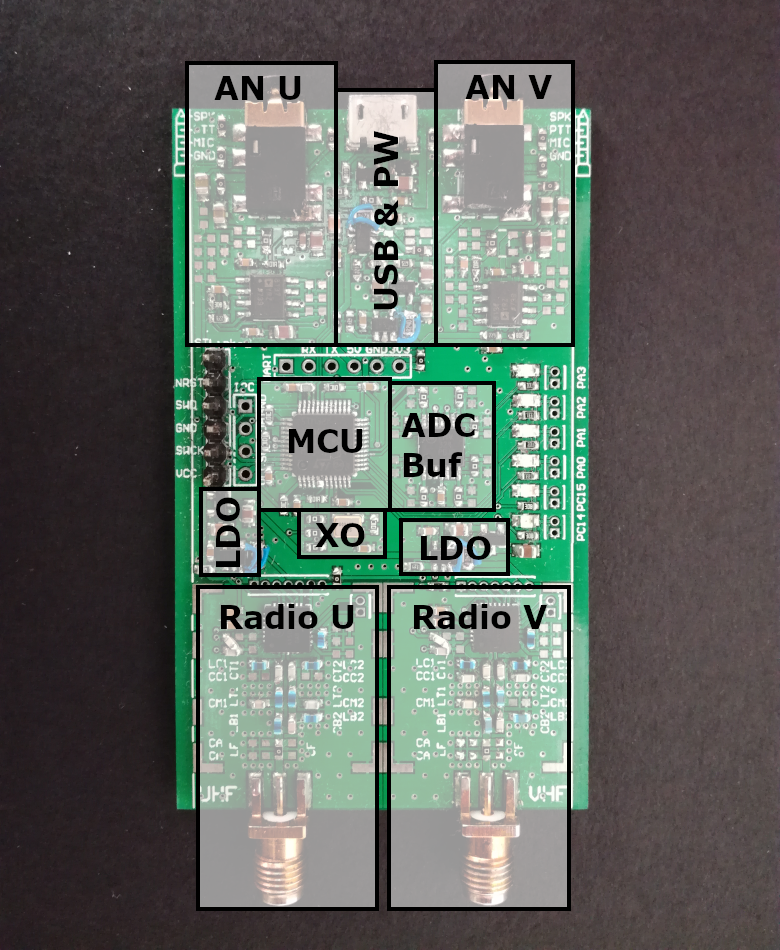
Power Domain
The module is powered from the USB port. The output of the USB is first down converted from 5V to 3.7V to improve efficiency. From there each power domain is powered from its own LDO, splitting the power into three separate domains. One for each of the Radios and one for the MCU and other ICs. This was done to improve noise isolation between these domains. Specially the radios, when emitting, can generate a lot of noise in the supply lines.
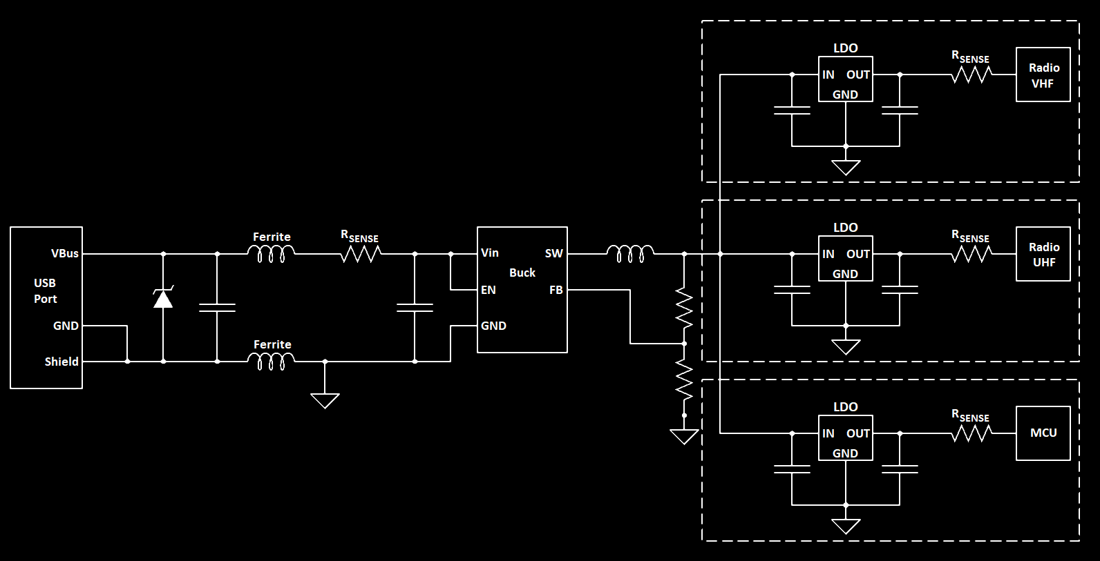
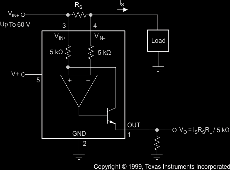
Each of these domains, as well as at the USB Power input, has a current sense circuit using the INA138. The current to voltage conversion gain of the INA138 is mainly determined by the load resistance, as can see in its datasheet:
So, to get a high voltage swing with a low sense resistor, to reduce the voltage drop across it, a high load resistor is needed. In the order of 100’s of kOhms. But with that the output can’t be directly connected to the STMs ADC input because the maximum recommended connected impedance is < 50kOhms, which goes down with increasing sampling rate. Therefore the output has to be buffered by an Op-Amp, in this case the TLV9004.
MCU and Clocks
The MCU used is the very popular STM32F103C8T6, often referred to as the blue pill. Called that for the Blue PCB module that is sold from Chinese sellers. This MCU has an integrated USB controller, perfect for this application, removing the need for a FTDI chip.
The MCU and radios use a shared XO of 16MHz as clock source. This will/can later be changed to a TCXO to improve clock accuracy and stability, especially useful for the transceivers. Each radio has a dedicated SPI interface to the MCU.
USB Interface
The main control and communication interface with the module is done over the USB Port. The USB Port is connected directly to the MCU. Each line has a diode clamping protection, with the power lines also having noise filtering using ferrite beads. Important to note that the STM32F103 USB controller does NOT have an internal pull-up resistor on the D+ line, this needs to be added externally. A 1.5kOhm pull-up to MCU Vcc (3.3 V) is recommended by STM. I found this out the hard way by not adding it in Version 2 and therefore spent a good amount of time debugging the not working USB connection… It appears that this is also a common problem with the blue pill boards, as some come with a wrong resistor value installed, 4.7k or even 10k, and can therefore cause issues if not replaced by the correct value.
Expansion Ports
The module features two expansion port connectors that can be used for future add-on modules and other expansions. One of the expansion ports is a UART interface, this is the port used to communicate with the Radio Interface add-on module. The other expansion port is a I2C interface that is currently not in use.
Status Indicator LED
There is a column of 6 LEDs that are connected through a series resistor to individual GPIOs of the Module and are used to indicate different Radio/Module status. The current meaning of each status LED is as follows, from top (PA3) to bottom (PC14):
- UHF Radio in transmission
- UHF Radio RSSI over threshold
- VHF Radio in transmission
- VHF Radio RSSI over threshold
- USB VCP Connected
- Module powered up
Radios
As explained before, the module is built around the AX5043, an Onsemi Sub GHz RF Transceiver. This is one of the most versatile and configurable single chip sub GHz transceivers out there. It supports the widest variety of modulations, including AFSK which is the whole point of this project.
Basic characteristics of the AX5043:
- Frequency range: 27 – 1050 MHz
- Output power: Up to 16 dBm
- Data-rates: 0.1 – 125 kBits/s
- Modulations: ASK, FM, AFSK, (G)FSK, (G)MSK, 4-FSK, PSK, O-QPSK
- Shared 256 bytes FIFO
Besides this it also handles HDLC frames: bit stuffing, flag framing and CRC calculation/validation. HDLC is used as the basis of AX.25 as explained on the dedicated HDLC/AX.25 page.
To achieve simultaneous VHF and UHF communications two of this chip are used. The circuits for each chip are the same, only the installed components vary. This transceiver provides a data interface trough two GPIOs, DATA and DCLK, which are connected to the MCU. It also has an analog input to the internal ADC and output from the internal DAC which are also connected and is explained below in section “Analog Interface”.
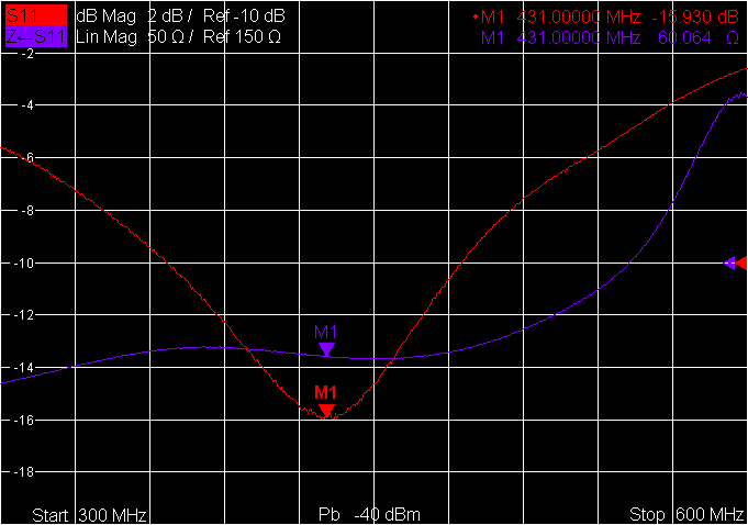
Matching Network
The RF connection to the transceiver uses the matching networks recommended in the datasheet and is using the differential input/output using the internal switching mechanism. This matching network in shown in the figure below.
The datasheet also provides values for all the components in the matching network for 4 different operation frequencies as shown in the table below. Although none of them match the desired frequencies exactly they are close enough to be used as a starting point.
| Freq. Band | LC1,2 (nH) | CC1,2 (pF) | CT1,2 (pF) | LT1,2 (nH) | CM1 (pF) | CM2 (pF) | LB1,2 (nH) | CB2 (pF) | CF (pF) | LF (pF) | CA (pF) |
|---|---|---|---|---|---|---|---|---|---|---|---|
| 169 MHz | 150 | 10 | 10 | 120 | 12 | NC | 68 | 12 | 6.8 | 30 | 27 |
| 433 MHz | 100 | NC | 4.3 | 43 | 11 | 5.6 | 27 | 5.1 | NC | 0 | NC |
| 470 MHz | 100 | NC | 3.9 | 33 | 4.7 | NC | 22 | 4.7 | NC | 0 | NC |
| 868 MHz | 18 | NC | 2.7 | 18 | 6.2 | 3.6 | 12 | 2.7 | NC | 0 | NC |
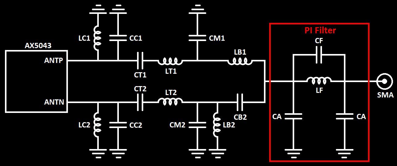
In the case for the VHF Band the PI filter is populated, as per the datasheet. The input matching (S11) with this PI filter can be seen in the figure below.
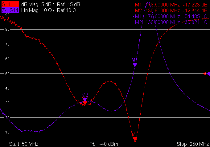
Two very close resonances are visible, one at around 131 MHz and one at around 179 MHz. The first resonances is created by the RX circuit of the transceiver. The second one is created by the PI filter. From this we can see that this filter is not designed for my desired frequency of 145.895 MHz. This makes sense when considering that the PI filter was specified for a frequency of 169 Mhz. Now it is possible to adjust the PI filter to the pretended frequency but I choose to remove it for now. With this the input matching is improved greatly but also results in a larger bandwidth. The input matching without the PI filter is shown below.
Without the PI filter a peak input reflection (S11) of -29.5 dB is achieved, at 155 MHz, with a -10dB bandwidth of 66 MHz (from 118 MHz to 184 Mhz). This means that at the frequency used, 145.895 MHz, the input reflection is well below -10 dB, which is great. The bandwidth is also reasonable considering no SAW is used.
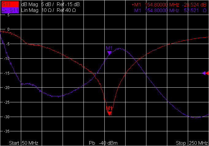
In case of the UHF transceiver no adjustments where necessary. In part because there is no PI filter used and because the given matching network values from the datasheet are closer to the desired center frequency (Datasheet: 433 MHz, Desired: 436.45 MHz) then in the VHF case. The input matching for the UHF transceiver is visible below.
A peak input reflection (S11) of -15.9 dB is achieved, at 431 MHz, with a -10 dBm bandwidth of 119 MHz (from 366 MHz to 485 MHz). Again we have a input reflection below -10 dB at the frequency used, 436.45 MHz. The bandwidth is larger then in the VHF case, almost double.
For the interested the S11 parameter files for the Hardware Version 2, the ones corresponding to the figures above, are available for download below:
VHF: VHF_S11.txt
UHF: UHF_S11.txt
And the S11 parameter files for the new Hardware Version 3 are also available below:
VHF: VHF_S11.txt
UHF: UHF_S11.txt
Analog Interface
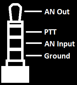
The transceiver has two analog interfaces, an input through an ADC and an output through a DAC. They are connected, with a signal conditioning circuit, to a 4-pole phone jack, one for each transceiver. The pinout of each 4-pole phone jack is identical and is shown in the figure below:
Analog Output
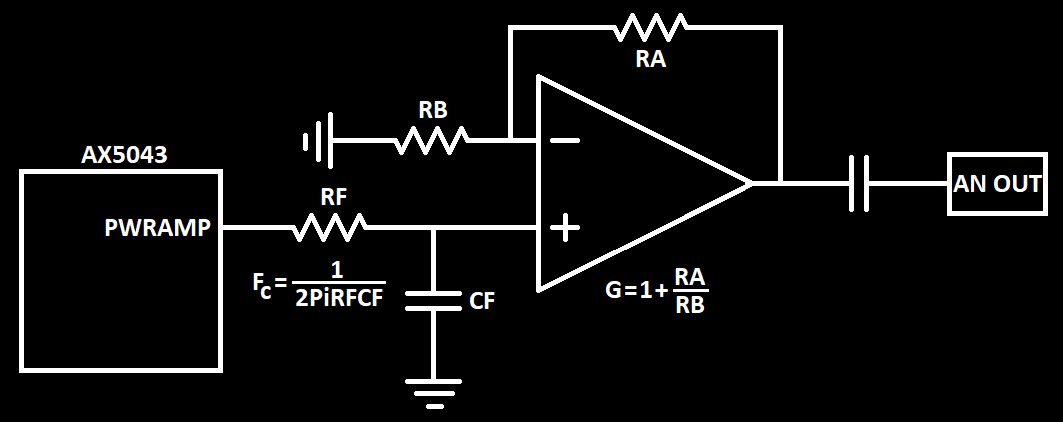
The DAC of the transceiver is not a “normal” DAC where the output is simply the desired voltage. It is a 1 bit DAC, meaning that the output has to be encoded and filtered so that different voltages are achieved. The DAC can be setup to output either a Sigma-Delta modulated signal or a PWM modulated signal. Normally the Sigma-Delta output should be selected as it has a much greater frequency range. The output Sigma-Delta has a base frequency of 16 Mhz (when using a 16 MHz clock source and using the frequency doubling) while the PWM has a frequency of only 7.8 kHz. The typical output of the DAC in Sigma-Delta mode looks like this:
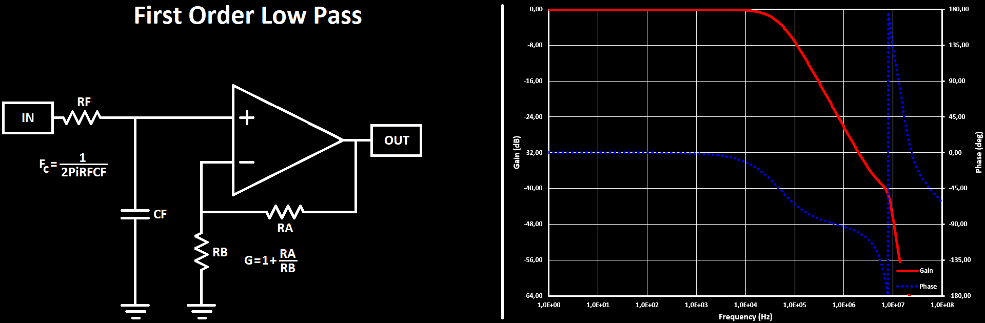
In the module the DAC output is mapped to the PWRAMP GPIO pin. This pin is connected to a simple RC first order low pass filter (LPF). This filter has a cutoff frequency given by $ F_c = {1 \over 2{\pi}RC} $ and has to be adjusted for different applications. For general use I used a $ F_c \approx 50 kHz $ by setting the resistor to 330 Ohm and the capacitor to 10 nF. The output of this filter is then fed into a buffer amplifier with a AC coupling capacitor to the phone connector output. This circuit is shown in the figure below:
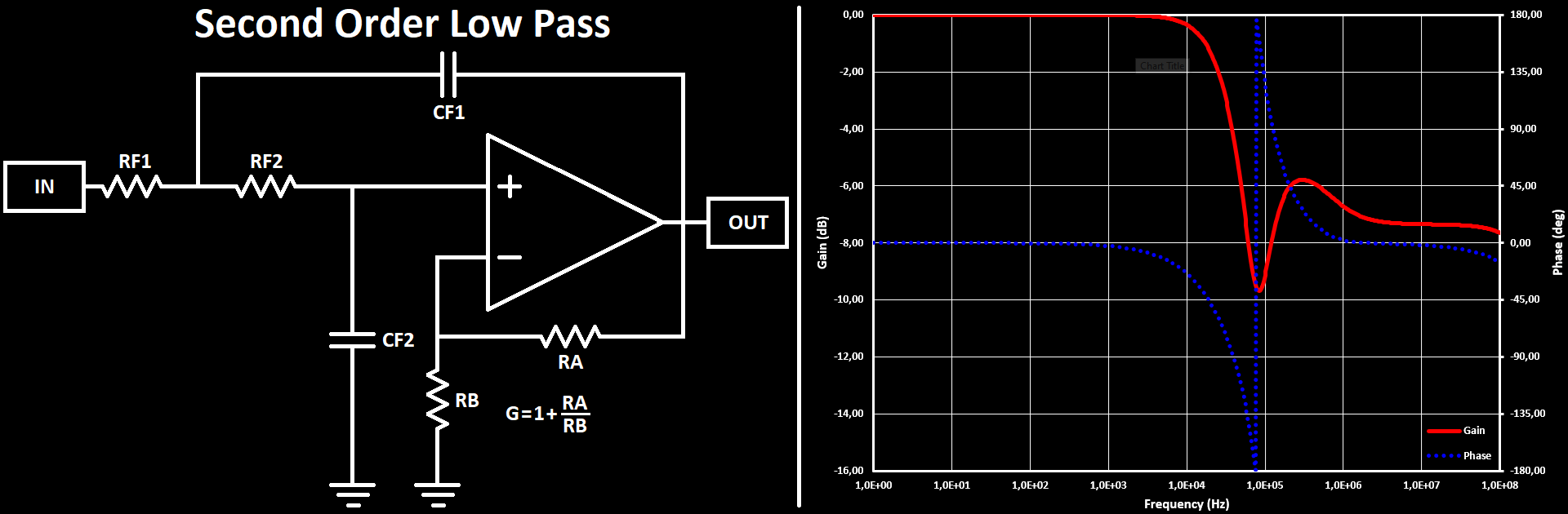
This filter is good enough for debugging and monitoring applications but when the DAC is used to output Audio it has to be improved for better audio quality. In Hardware Revision 3, an active second order LPF was added (Sallen-Key Topology), replacing the simple first order RC filter. During testing of the new filter it was observed that the output signal was worse then with the simple RC filter, which was not expected with the new higher order filter. It turns out that the Sallen-Key topology has a well know drawback of large high frequency feedthrough.
At high frequency the OpAmp output impedance increases substantially, and the input signal jumps straight to the output through the feedback capacitor… This was also observed in Spice simulations but in practice it was even worse with almost zero attenuation of the DAC pulse modulation. The filter therefore had to be changed again and it was switched to a double RC filter, mainly because it fit the already existing hardware well. This new filter is also a second order filter but without the feedthrough problem, improving the DAC pulse modulation rejection significantly. The used value for the capacitors is 2 nF and the resistors 560 Ohm giving a $ F_c \approx 50 kHz $. It is the filter used in all experiments with Audio outputs, FM and AM demodulations.
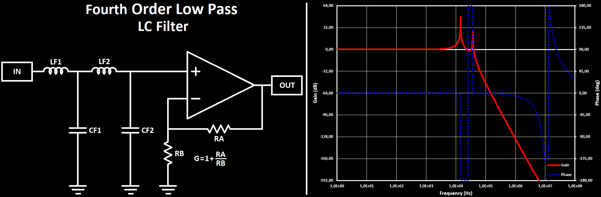
To improve the filter performance further, while still keeping the current hardware design, another implementation was tested using an LC ladder filter instead of the RC filter, replacing the resistors with inductors. The resulting LC filter is a second order low pass (resonator) filter and with two in series it is effectively a forth order LPF. The filter gave promising results in simulations, but after implementation a new problem was discovered, which was not evident in a AC simulation in Spice, the impedance of the LC filter decreases with frequency and gets close to 0 very fast, effectively shorting the DAC output to ground (obvious in hindsight). With the used component values of 22uH and 2.2uF, giving a $ F_c \approx 40 kHz $, the impedance goes to almost 0 at frequencies above 1kHz, effectively decreasing $ F_c $ to 1 kHz. The problem in the implementation used is the missing source (RS) and load (RL) resistors in the LC ladder, the addition of those would solve the problem but it complicates the integration in the current hardware and was therefore dropped for the double RC filter.
Below is a comparison of all 4 filter designs used, with their respective circuit and simulation results of their frequency response.
Analog Input
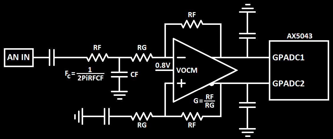
The ADC of the transceiver that is used for the baseband signal sampling in the RX chain also has one multiplexed input mapped to the GPIO pins GPADC1 and GPADC2. The ADC has 10 bits with a maximum sampling rate of 1 MS/s and differential inputs with 50 kOhm input impedance. The common mode voltage (center voltage) is 0.8V and the input voltage range is from -500mV to 500mV. The ADC can also be used in single ended mode, with the GPADC2 pin connected to ground.
For this module the differential mode is used. The analog signal is connected from the phone connector through a AC coupling capacitor to a simple RC first order low pass filter, just like the DAC. Again this filter has to be adjusted for different applications. The output of the filter is then connected to a differential amplifier that converts the single ended input signal to a differential signal with a common mode voltage of 0.8V. When using the differential amplifier in this way, with AC coupled input, it is important to not forget to add the AC coupling capacitor in the feedback loop! This signal is then connected to the transceivers ADC input pins. This circuit can be seen in the figure below:
Costume drivers for both the Radio and the MCU peripherals where developed, with exception to the USB stack for the MCU. The peripheral drivers use the Low Level libraries from STM. For the USB stack the library provided by STM is used.
The communication protocol used to control the Module, both over USB and UART, is based on CAT commands used by some HAM Radios like from YAESU or Kenwood. It is not compatible with those commands as the module is very different in its operation, it has digital demodulation amongst other differences, but the commands are mirrored as closely as possible. Below is a pdf with all the currently implemented commands, this is a evolving command interface with many changes expected:
CAT Commands: VUHF_Radio_CAT_Commands.pdf
When using the digital modulations the Module both the USB and UART interfaces not only carry the CAT commands but also the RX and TX packets. The packets are transferred over these interfaces using a common low level TNC protocol called KISS. This means that for digital modulations, both the UART and USB interface carry two different communication protocols, which allows to both receive and transmit packets as well as controlling all the Modulation/RF parameters of the module at the same time.
Explanation on how to program/configure the AX5043 transceiver can be read in it’s dedicated page, where I try to explain as best as possible the steps to set up the transceiver using this projects set-up as examples.
The full software is available on Github: VUHFRadio
This section is dedicated to showing the practical results obtained with this module.
Power Consumption
The power consumption of the whole module for different scenarios/modes are listed in the tables below:
For the UHF Radio:
| Radio Mode | Pout (dBm) | I VHF (mA) | I MCU (mA) | I Global (mA) |
|---|---|---|---|---|
| Power Down | NA | 0.5 | 42 | 42 |
| RX | NA | 15 | 42 | 61 |
| TX: AFSK 1200 | 15.8 | 46 | 42 | 90 |
| TX: MSK 9600 | 15.8 | 46 | 42 | 93 |
For the VHF Radio:
| Radio Mode | Pout (dBm) | I VHF (mA) | I MCU (mA) | I Global (mA) |
|---|---|---|---|---|
| Power Down | NA | 0.5 | 42 | 42 |
| RX | NA | 11 | 42 | 61 |
| TX: AFSK 1200 | 14 | 87 | 42 | 127 |
| TX: MSK 9600 | 14 | 87 | 42 | 124 |
With this result we can calculate the radio efficiency in TX mode. For UHF it results in 19.2% and for VHF in 18.5%. This values are far from the 50% efficiency given in the datasheet. This lower efficiency is due to the 50% efficiency from the datasheet is only for the PA, not taking into account other parts, and when the PA is powered from 1.8V and not from 3.3V like in this module and therefore is downconverted to 1.8V by an internal LDO.
TX Results
The modulations that are working and tested are AFSK, (G)MSK and BPSK. The results for both in VHF and UHF are very similar and therefore only figures for the UHF case are shown. Also, the configurations of the transceiver used are the ones explained in the AX5043 page, with the TX power set to the maximum.
The maximum measured output power (programmed to the maximum of 16 dBm) is over 14dBm for both tested modulations, giving a 2dBm loss in the matching network circuit.
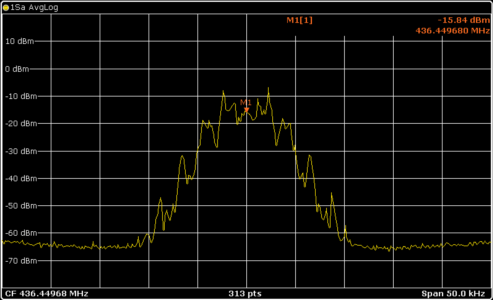
The output spectrum in AFSK-1200 mode, AFSK @ 1200 bits/s and FSK deviation of 3000 Hz, is visible below:
And below is a short clip showing the AFSK-1200 modulation being received and demodulated on the PC using an RTL.SDR with SDR# as the FM Receiver that outputs to the SoundModem TNC Software for demodulation and displaying the frame. This set-up is equivalent of using a HAM Radio with a TNC as receiver and demonstrates that the VUHFRadio Module is compatible with those.
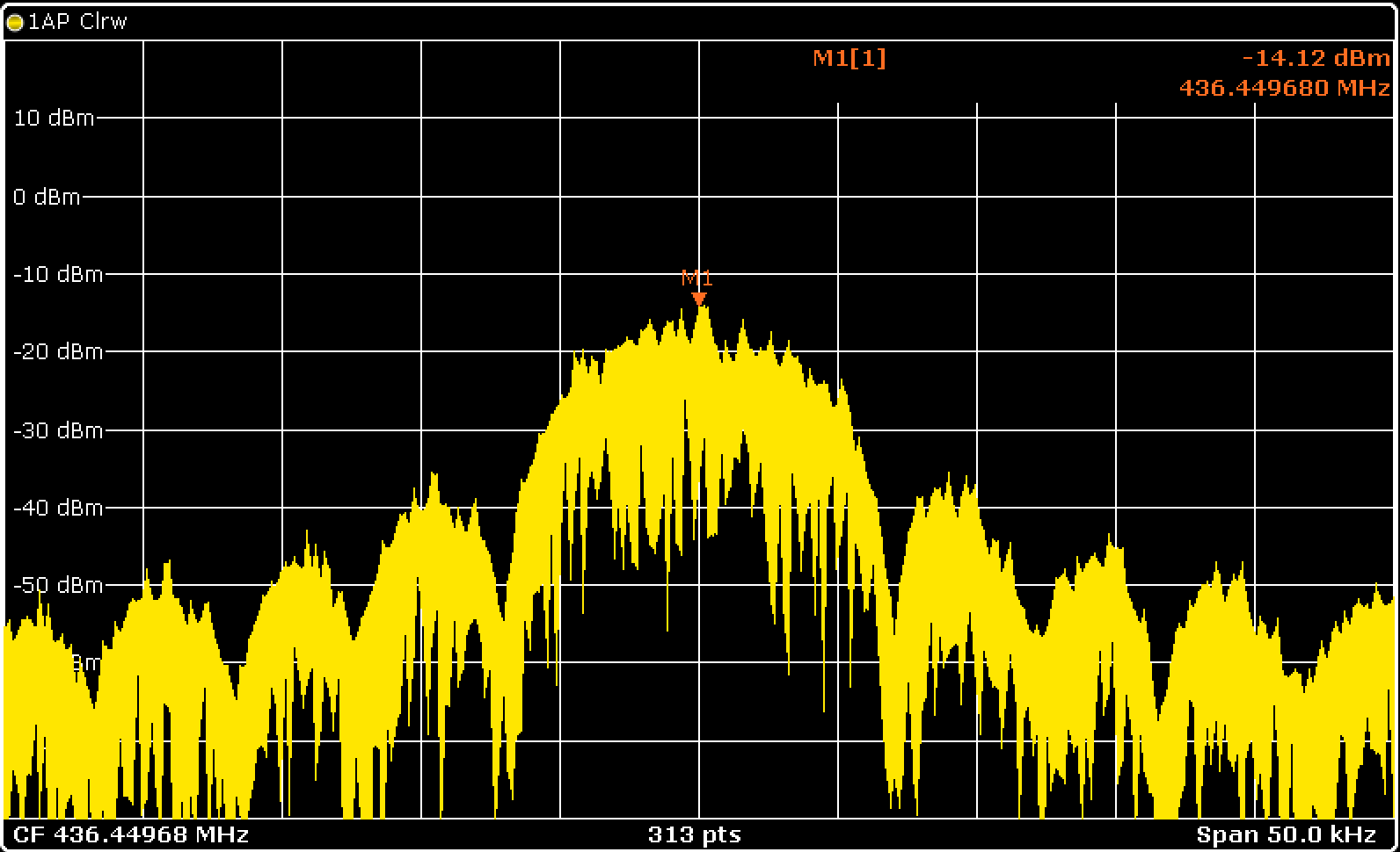
And the output spectrum in MSK (G3RUH) mode @ 9600 bits/s and FSK deviation of 4800 Hz, is visible below:
And again, below is a clip of this modulation being received and demodulated on the PC, with the same set-up as the above AFSK-1200 set-up but using the SoundModem HS.
Both these modulations have a very clean spectrum, matching the ideal spectrums very well.
Getting PSK/BPSK to work was more difficult due to a missing register description in both the datasheet and programming manual. The MODCFGP (0xF5F), the register that controls PSK settings, great… I finally found the needed information in a blog post from On Semiconductors, would be great if that info was in the documentation. The AX-RadioLAB configures that register appropriately. With this information it is trivial to make BPSK Modulation work, based on the previous modulation.
The figure below shows the output spectrum in BPSK mode @ 9600 bits/s.
RX Results
Currently the working demodulations are AFSK-1200 and (G)MSK-9600. All test results shown here are using the configurations explained in the AX5043 page with the exception of when changes in those configurations are tested.
The first test performed was checking the accuracy and calibrating the RSSI value returned by the transceiver. For the UHF transceiver the RSSI value was about 11 dBm above the real input power and had to be calibrated by setting the RSSIREFERENCE register to -11. This register is there for this, to compensate for board effects. For the VHF transceiver this calibration value is also -11.
Next the BER performance of the AFSK-1200 demodulation was tested. To perform the BER test a continuos stream of 0s are passed through a scrambler and NRZI encoder which gives a good randomization, needed for accurate testing. This bitstream is then modulated and transmitted, using an ADALM-PLUTO SDR, to the Module. On the Module side, the transceiver is setup to output the demodulated, unscrambled and decoded bits on the DATA/DCLK lines which are monitored by the MCU. When all is correct, no bit errors, a continuos stream of 0s should be observed, any 1s represent a bit error. To note that the scrambling has an error multiplication factor equal to the number of feedback taps, here 3. The NRZI encoding also has an error multiplication factor, in this case of 2. This gives a global error multiplication factor of 6, meaning that the number of 1s measured by the MCU is 6 time higher then the actual number of wrong bits.
The results of the BER test for AFSK-1200 in UHF are shown in the table below, where the error multiplication factor is already taken into account. A variable attenuator was used in the chain and the input power (Pin) of the module was measured with a signal analyzer, measuring the channel power with a BW equal to the RX BW of the transceiver. For a good BER estimate a minimum of 30 bit errors have to be observed.
| Attenuation (dBm) | Pin (dBm) | RSSI (dBm) | #Bit Errors | #Bits | BER |
|---|---|---|---|---|---|
| 0 | -22.2 | -30 | 0 | 3031028 | >10-5 |
| 10 | -31.3 | -34 | NA | NA | NA |
| 20 | -41.3 | -42 | NA | NA | NA |
| 30 | -51.4 | -51 | NA | NA | NA |
| 40 | -61.2 | -63 | NA | NA | NA |
| 50 | -71.4 | -72 | NA | NA | NA |
| 60 | -81.6 | -81 | NA | NA | NA |
| 70 | -91.4 | -90 | NA | NA | NA |
| 80 | -102.5 | -101 | 0 | 3003073 | >10-5 |
| 85 | -106.6 | -107 | 51 | 2839277 | 1.8x10⁻⁵ |
| 90 | -111.6 | -116 | 1935 | 301038 | 6.4x10⁻⁵ |
From this table it is visible that after calibration the RSSI value of the transceiver is very close to the real one, only at -22dBm input power there is a big difference and which is a very uncommon situation anyways. For input powers above -105 dBm the BER is over 10-5. I didn’t want to wait until I get 30 bit errors, which could take hours, and stopped when it was clear that it was over 10-5 by receiving at least 30x105 bits with no errors.
The same BER test was also performed for GMSK-9600 with a BT of 0.5, with the results for the UHF transceiver shown in the table below:
| Attenuation (dBm) | Pin (dBm) | RSSI (dBm) | #Bit Errors | #Bits | BER |
|---|---|---|---|---|---|
| 0 | -20.8 | -28 | NA | NA | NA |
| 10 | -29.8 | -28 | NA | NA | NA |
| 20 | -39.6 | -38 | NA | NA | NA |
| 30 | -49.7 | -47 | NA | NA | NA |
| 40 | -59.6 | -59 | NA | NA | NA |
| 50 | -69.7 | -68 | NA | NA | NA |
| 60 | -80.0 | -79 | NA | NA | NA |
| 70 | -90.0 | -85 | 0 | 3006194 | >10-5 |
| 80 | -101.0 | -96 | 2 | 4632745 | >10-5 |
| 85 | -106.4 | -102 | 60 | 1878145 | 3.2x10⁻⁵ |
| 90 | -110.6 | -106 | 17351 | 505266 | 3.4x10⁻² |
The performance is very similar to AFSK-1200 for input powers over -105 dBm, with a BER over 10-5.At the lowest tested power level the BER performance is much worse then for AFSK-1200, this is not expected as the required SNR for GMSK-9600 is lower then for AFSK-1200 and is likely do to testing inaccuracies.
Both BER tests where also performed for the VHF transceiver with the results shown in the tables below.
For AFSK-1200:
| Attenuation (dBm) | Pin (dBm) | RSSI (dBm) | #Bit Errors | #Bits | BER |
|---|---|---|---|---|---|
| 0 | -25.5 | -30 | NA | NA | NA |
| 10 | -32.4 | -31 | NA | NA | NA |
| 20 | -42.4 | -42 | NA | NA | NA |
| 30 | -52.5 | -51 | NA | NA | NA |
| 40 | -62.4 | -63 | NA | NA | NA |
| 50 | -72.5 | -72 | NA | NA | NA |
| 60 | -82.8 | -81 | NA | NA | NA |
| 70 | -92.7 | -89 | 2 | 3002802 | >10-5 |
| 75 | -97.1 | -93 | 425 | 1311193 | 3.2x10⁻⁴ |
| 80 | -102.7 | -97 | 267 | 124733 | 2.1x10⁻³ |
| 85 | -107.1 | -100 | 10057 | 161809 | 6.2x10⁻² |
And for GMSK-9600:
| Attenuation (dBm) | Pin (dBm) | RSSI (dBm) | #Bit Errors | #Bits | BER |
|---|---|---|---|---|---|
| 0 | -23.7 | -30 | NA | NA | NA |
| 10 | -30.8 | -28 | NA | NA | NA |
| 20 | -41.6 | -38 | NA | NA | NA |
| 30 | -51.0 | -47 | NA | NA | NA |
| 40 | -61.1 | -59 | NA | NA | NA |
| 50 | -71.0 | -68 | NA | NA | NA |
| 60 | -81.1 | -78 | NA | NA | NA |
| 70 | -91.3 | -85 | 2 | 3004398 | >10-5 |
| 75 | -96.4 | -89 | 30 | 1940245 | 1.5x10⁻⁵ |
| 80 | -101.2 | -94 | 1285 | 505715 | 2.5x10⁻³ |
| 85 | -105.4 | -98 | 10166 | 306756 | 3.3x10⁻² |
From this it can be seen that the performance of the VHF transceiver is worse then the UHF one. I don’t know why this is but it is very clear and visible for both modulations.
Another test that was performed was changing the receiver BW and seeing the impact of this on the BER. This test was performed using the GMSK-9600 modulation on the UHF transceiver using a 80 dBm attenuation, -100 dBm input power, and a 85 dBm attenuation, -105 dBm input power. The results are shown in the Tables below:
Attenuation of 80 dBm, -100 dBm input power:
| BW (kHz) | RSSI (dBm) | #Bit Errors | #Bits | BER |
|---|---|---|---|---|
| 14.4 | -97 | 2 | 4632745 | >10-5 |
| 28.8 | -99 | 0 | 3008934 | >10-5 |
| 57.6 | -98 | 5 | 3006816 | >10-5 |
| 115.2 | -111 | 67 | 1532975 | 4.4x10⁻⁵ |
Attenuation of 85 dBm, -105 dBm input power:
| BW (kHz) | RSSI (dBm) | #Bit Errors | #Bits | BER |
|---|---|---|---|---|
| 14.4 | -102 | 60 | 3180917 | 1.9x10⁻⁵ |
| 28.8 | -104 | 60 | 542033 | 1.1x10⁻⁴ |
| 57.6 | -103 | 884 | 505601 | 1.7x10⁻³ |
| 115.2 | -117 | 6824 | 507738 | 1.3x10⁻² |
The results are as expected, with increasing BW the BER gets worse, confirming that using the smallest BW possible is very important.
AM Audio Demodulation
Over at Hackaday, a member asked me if it was possible to use the transceiver as a basic Audio AM demodulator which sparked my interest as I remembered that the transceiver could output many different tracking variables on its DAC. One of those variables is the amplitude tracking information, which is exactly what is needed to output an AM demodulated audio signal. This functionality is the basis for using this transceiver as a simple AM receiver. Modulation is, as far as I can tell, not possible.
For this, the first thing to do is to configure the internal DAC to output the amplitude tracking information. This is done by setting the DACCONFIG (0x07) register to 0x01 (TRKAMPLITUDE). The DACSHIFT bits in the DACVALUE registers (0x330-0x331) should be set to 0x0C and using the DAC in $ \Sigma\Delta $ mode is required. The DAC output, as discussed before, has to be low pass filtered, preferably with a high order filter as will be seen later.
The next step is to set the $ F_{Center} $ while taking into account that for the amplitude tracking to work the IF stage of the receiver has to have a signal with the amplitude modulation. With the settings used here the best working IF frequencies where in the 2 kHz to 6 kHz range. This means that the programmed $ F_{Center} $ has to be 2 kHz to 6 kHz below (or above) the transmitted signal frequency. As an example, for a programmed $ F_{Center}=436.449 MHz $ the modulated input signal has to fall in one of the following ranges:
- Lower Range: 436.447 MHz to 436.443 MHz
- Upper Range: 436.451 MHz to 436.455 MHz
Another consequence of this is that the AFC function has to be disabled as it will try to correct the $ F_{Center} $ and therefore can change the IF frequency to outside the usable range. To disable the AFC the MAXRFOFFSET (0x109-0x10B) register is set to 0x00.
With this set up, the IF Filter (Decimation) and RX Datarate can be configured. The RX Datarate sets the sampling frequency of the IF signal and therefore has to be set high enough to sample the 2 kHz to 6 kHz IF signal so that the amplitude tracking works well. From my observations the sampling frequency seems to be slightly above the set RX datarate (~1.2x higher). The RX Datarate used is 200 kbits/s and the IF filter bandwidth is set to 50 kHz (decimation set to 20). Both the IF frequency setting (IFFREQ), which only affects the second IF frequency, as well as what demodulation is used doesn’t seem to affect the amplitude tracking performance (AM demodulation). FSK is used as the demodulation (modulation) setting and the IF frequency is set to 25 kHz.
Finally, both the AGC as well as amplitude processing have to be configured. The AGC is set to the slowest possible setting without disabling it so to not distort the AM signal. This is done by setting the AGCATTACK0 and AGCDECAY0 bits of the AGCGAIN0 (0x120) register to 0x0E. The AGC target amplitude (AGCTARGET0) is set to 192, a bit below the mid-range, which gives a good range for the amplitude variations from the AM modulation without saturations. The Amplitude gain register (AMPLGAIN0) is set to 0x04, which trough experimentation gave the best results. Playing with both the AGCTARGET0 and AMPLGAIN0 values changes the demodulated audio signal quality significantly.
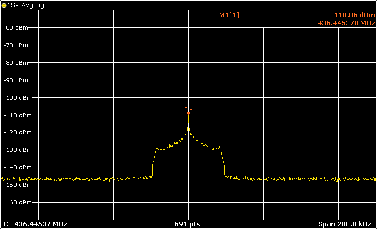
To generate the AM signal, a signal generator is used with the external modulation source input connected to the audio output of a computer. The following settings were used for the signal generator:
- Frequency: 436.444500 MHz
- Output Power: -70 dBm
- AM Source: External Audio (<500mV p-p)
- AM Type: Exponential
- AM Depth: 25 dB (25 dB/V Sensitivity)
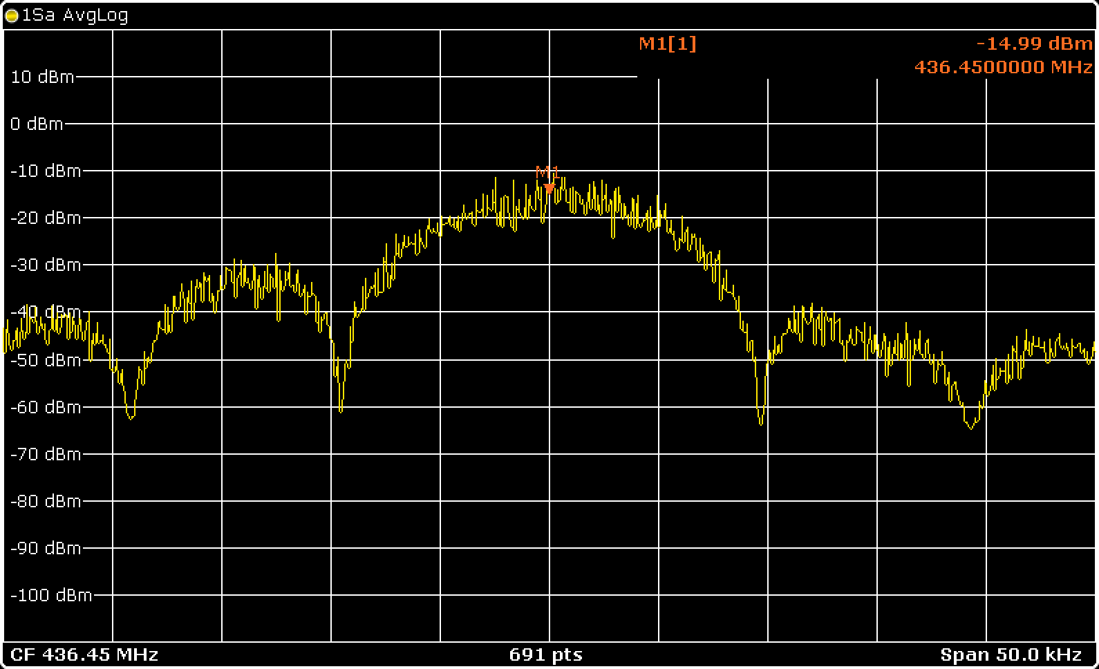
These settings give a AM modulation index of around 50%, which gave the best results. This limitation are due to a combination of the signal generator and the transceiver. The signal spectrum generated by a white noise audio source is shown in the figure below..
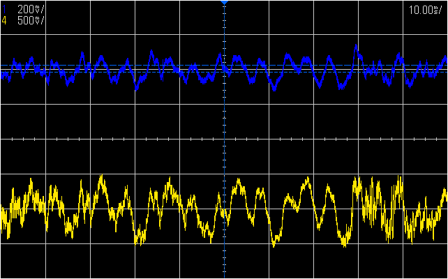
Below the AM modulated IF signal at the transceiver is visible, in blue, as well as the original audio source, in yellow. This is the output of the DAC when either SAMPLE_ROT_I or SAMPLE_ROT_Q is used as the DAC input. This is useful during debugging to see if there is a IF signal and what the frequency and amplitude of it is. When zoomed in, the IF sine wave would be visible with a frequency between 2 kHz and 6 kHz.
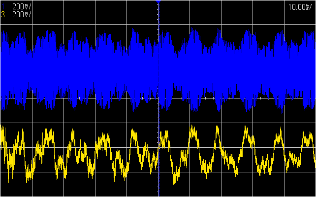
The amplitude tracking information, demodulated AM signal, output by the DAC can be seen in the figure below in blue, with the original audio source shown in yellow:
From this figure it is visible that the original audio signal is indeed being demodulated and output by the transceiver! But it is also visible that it is involved in a lot of noise, which is also very audible. Below is a recording of the demodulated audio output from the module, it starts around the 30s mark:
The audio recording from above was recorded directly from the audio jack of the module with no further post-processing. A standard headphone can be plugging into this jack to listen to the AM demodulated audio. Only on one side of the headphones though as it is a mono output and demodulation. This is actually much better audio quality than was expected, I didn’t even expect to be able to get AM demodulation working at all.
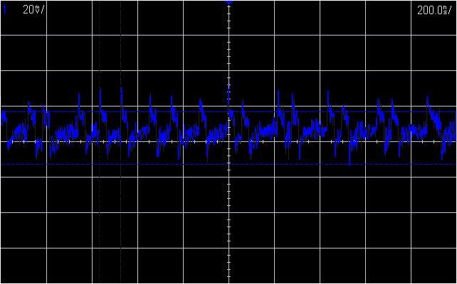
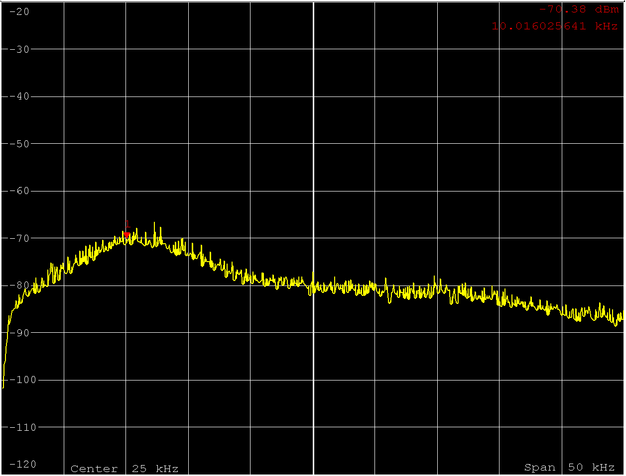
Further analysis of the noise shows that the main source of it is the DAC modulation that is not filtered very well even when using the dual RC, second order, low pass filter, with a $ F_C = 25 kHz $. The figure below shows this noise where the $ \Sigma\Delta $ modulation of the DAC is still very visible:
Below is the spectrum of this noise, which shows that it is concentrated around 10 kHz explaining why the demodulated audio has much better clarity in the low frequencies (Bass).
This shows that improving the DAC output filtering can significantly improved the audio quality. This was also observed when switching from a simple RC, first order, low pass filter to a dual RC, second order, low pass filter, reducing the noise from ~10 mV RMS to ~7 mV RMS. Further tuning and experimentation with the transceiver settings also promises to improve the AM demodulation and the audio quality.
FM Audio Demodulation
Analog FM demodulation, and modulation, is a unique and officially supported special feature of this transceiver. Onsemi even provides an application note on how to set up and use the transceiver as an analog FM transceiver, “AX5043 Use as Analog FM Transceiver”. The application node is used as the basis for this section.
There are two common FM modulations used, Wideband FM (WBFM) and Narrowband (NBFM). They differ mainly in the frequency deviation used and therefore the occupied bandwidth. The Table below shows the characteristics and differences between WBFM and NBFM.
| WBFM | NBFM | |
|---|---|---|
| Modulation Index | greater then 1 | less then 1 |
| Frequency Deviation | less then 75 kHz | less then 5 kHz |
| Modulating Frequency | 30 Hz - 15 kHz | 3 kHz |
| Bandwidth | over 100 kHz | 15 - 20 kHz |
| Application | FM Radio Broadcast | Voice Communications |
As with AM demodulation, the first thing is to set up the DAC output, here the frequency tracking value should be used as the DAC output. This is done by setting the DACCONFIG (0x07) register to 0x03 (TRKFREQUENCY). The other DAC settings are the same as for the AM demodulation mode. Next, the modulation/demodulation mode has to be set to FM (0x08) in the MODULATION (0x010) register and the RF center frequency is programmed, to the center frequency of the FM signal. The RF bandwidth is set with the DECIMATION register, as with all modulations, while the sampling rate of the demodulated FM signal is controlled by the RXDATARATE register where the RX datarate (BITRATE) is now the sampling rate, $ F_s $. The IF frequency (IFFREQ) is set to 20 kHz (can be another value but this is the value used here and can serve as a reference value). AFC can be used or be disabled, if AFC is enabled the frequency correction has to be preformed at the first LO and with the lowest tracking speed/bandwidth (FREQGAIND0).
The RXPARAMSETS register should be set to 0x00 to ensure that only the RX parameters 0 are used, at all times. As in the AM mode, the AGC attack speed is set to the slowest response by setting the AGCATTACK0 bits of the AGCGAIN0 (0x120) register to 0x0E. The decay speed (AGCDECAY0) is set to a slightly faster response, set to 0x0A, to prevent peaking. The target magnitude (AGCTARGET0) is set to 0x80. Both the timing and datarate recovery loops are disabled by setting both the TIMEGAIN0 (0x124) and DRGAIN0 (0x125) registers to 0x00. The frequency gain registers are set as shown in the table below and as is described in the application note:
| Register | Value | Note |
|---|---|---|
| FREQGAINA0 (0x127) | 0x0F | Off |
| FREQGAINB0 (0x128) | 0x04 | Bandwidth of “inner” AFC loop used for FM demodulation. F3dB = 0.115*BR |
| FREQGAINC0 (0x129) | 0x1F | Off |
| FREQGAIND0 (0x12A) | 0x08 | Bandwidth of “outer” AFC loop (tracking frequency mismatch) |
From those, the most important register is FREQGAINB0 (0x128), which controls the bandwidth of the demodulated FM signal. The relation between the register value and the bandwidth is not given by Onsemi and was obtained through experiments. The bandwidth seems to be given by:
$$ F_{3dB} = { BITRATE \over 2 } * 2^{-FREQGAINB0} $$
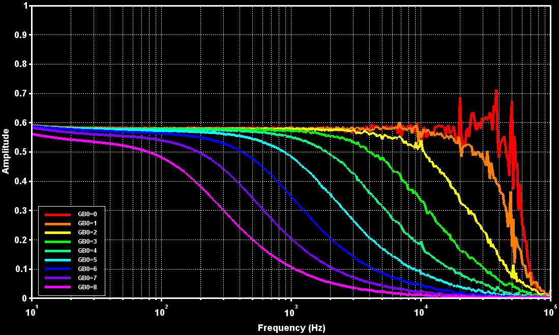
The experiment done to arrive at this formula was to measure the frequency response of the demodulated FM signal (DAC output). This was done by connecting a network analyzer to the RF signal generator external modulation input and to the DAC output. The experiment was performed for both WBFM and NBFM, with the RF signal generator set to a FM sensitivity of 75 kHz/V and 2.5 kHz/V respectively. The settings used for the VUHFRadio in WBFM were a DECIMATION value of 2 and a $ F_s $ of 200 ksps (RXDATARATE set to 5120), while for NBFM a DECIMATION value of 16 and a $ F_s $ of 31.25 ksps (RXDATARATE set to 4096) was used. The results can be see in the figures below:
The difference in the base gain/amplitude of the output demodulated FM signal is due to the set receiver FM sensitivity (kHz/V), which is given by the formula below and depends on $ F_s $ (taken from the programing manual as the meaning of the TRKFREQUENCY register):
$$ \Delta F = { TRKFREQUENCY \over 2^{16} } * BITRATE $$
Taking into account that the TRKFREQUENCY register is directly output to the DAC and that the DAC has a maximum output amplitude of 1.65 V ($ \sigma \delta $ and VDDIO of 3.3 V), we can rewrite the formula as follows (with DACSHIFT set to 0x0C):
$$ Sensitivity = {1 \over 1.65} * {BITRATE \over 2} $$
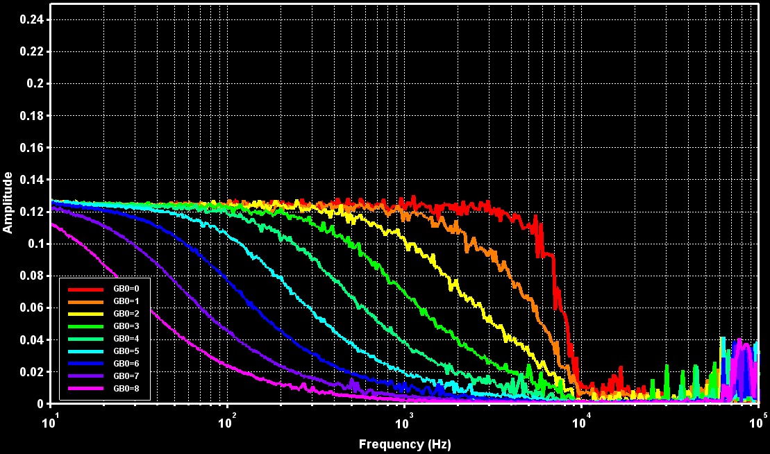
This shows that the FM deviation, the FM receiver sensitivity, is set by the sampling rate ($ F_s $). This was also verified experimentally by changing only the RXDATARATE register, changing $ F_s $, and observing the change in the output amplitude of the demodulated FM signal with a 1 kHz signal feed into the RF signal generator (reference signal). This was again performed for both NBFM and WBFM with the same settings as in the previous experiment. The results are shown in the figure below:
This poses a problem for narrowband FM where the sensitivity should be around 2.5 kHz/V meaning that $ F_s $ (BITRATE) should be set to 8250 but this is a very low value and will not give a good audio quality… The problem can be mitigated somewhat by decreasing the DACSHIFT register value, effectively adding digital gain to the DAC output. Decreasing the shift by one doubles the usable bitrate without decreasing the output amplitude. This comes with the tradeoff of increased noise in the output signal.
Results for WBFM
With the VUHFRadio in WBFM mode, configured as in the above tests, the FM demodulation was tested with actual FM modulated audio. The first tests where performed with a RF signal generator where the external modulation source input is connected to the audio output of a computer. The following configurations are used for the RF signal generator:
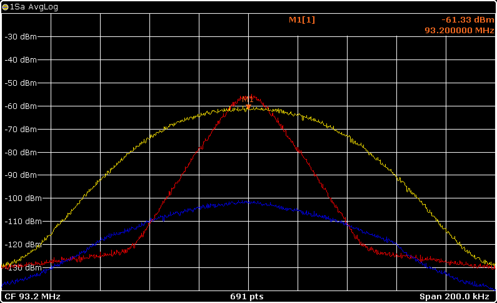
- Frequency: 93.200 MHz
- Output Power: -70 dBm
- FM Source: External Audio (<500mV p-p)
- FM Mode: Normal
- FM Deviation: 75 kHz (75 kHz/V Sensitivity)
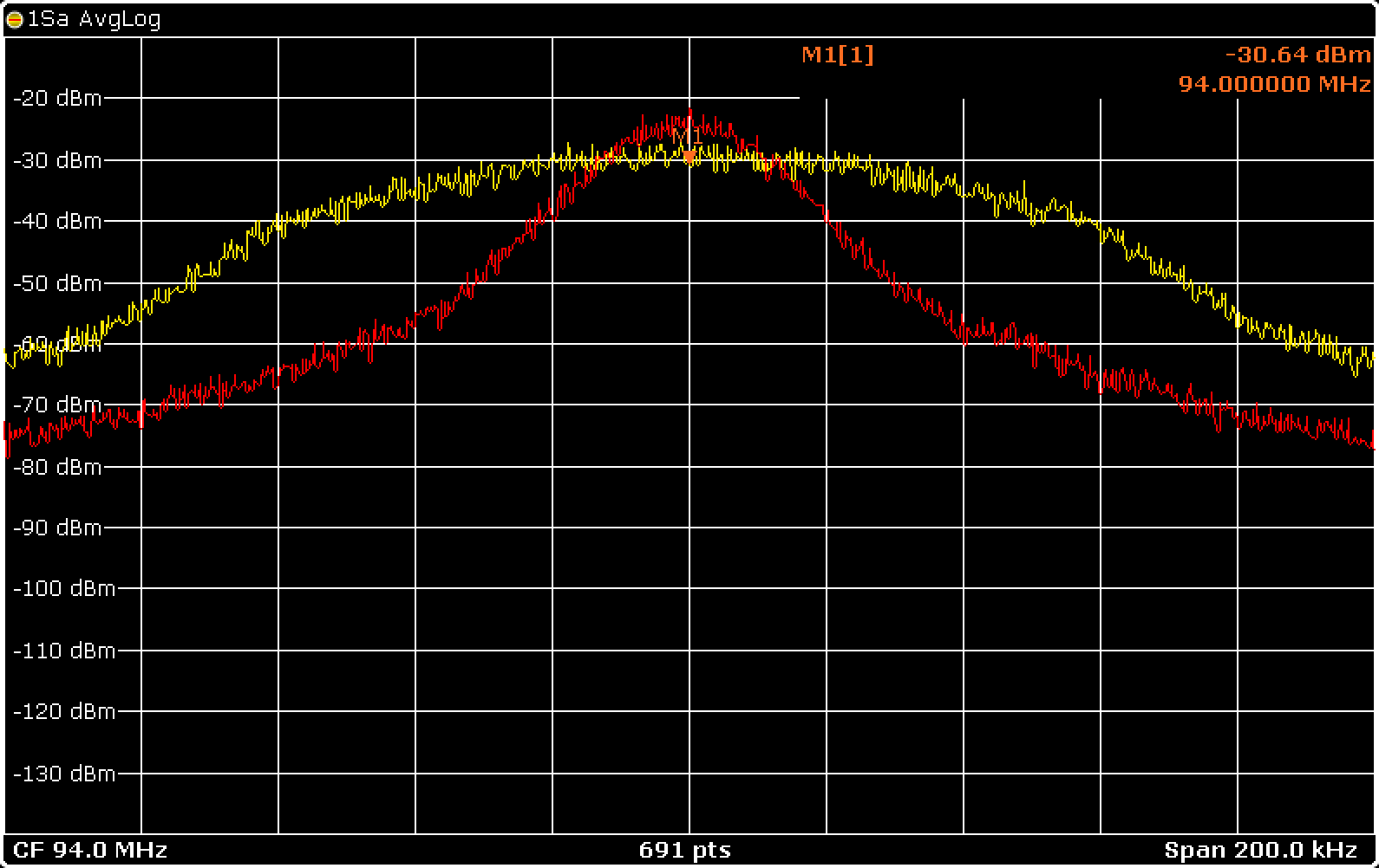
The figure below shows the spectrum generated when using a white noise audio file as the source, this generates the “purest” and widest spectrum. In yellow is the spectrum of this when using 100% volume (~1Vp-p), and in red when using 50% volume (~400mVp-p). In blue is the spectrum of a FM radio station for comparison.
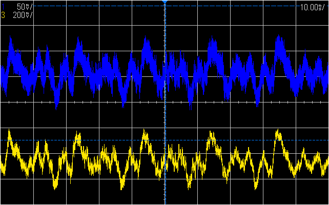
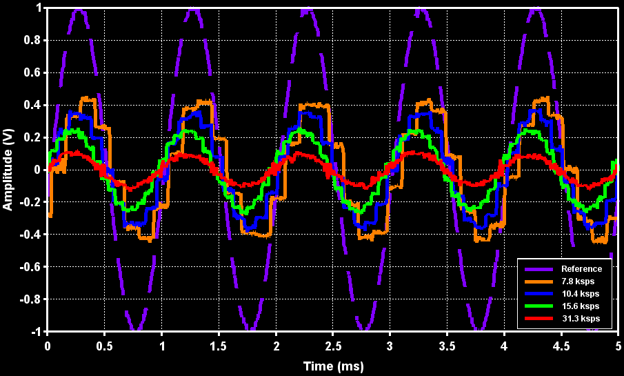
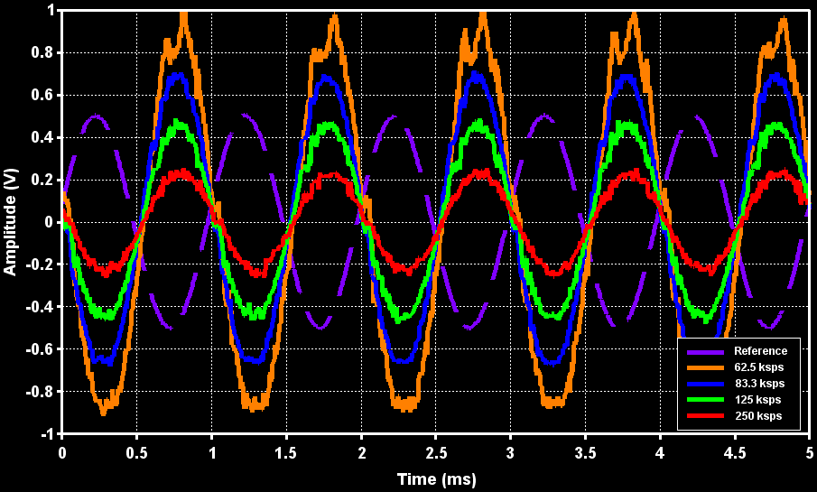
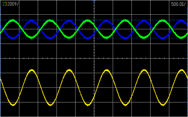
Below is a figure showing the FM modulated signal at the IF stage of the transceiver, with a audio file as the modulation source, shown in blue. The original audio source is shown in yellow. This is the output of the DAC when either SAMPLE_ROT_I or SAMPLE_ROT_Q is used as the DAC input.
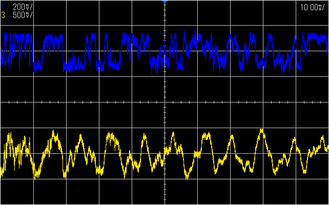
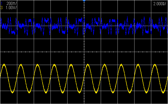
The FM modulation is not very clearly visible in this figure because it is a composition of a complex signal. To see the FM modulation better, at the IF stage of the transceiver, a single tone is used as the modulating audio source. The result is shown in the figure below, in blue again the FM modulation at the IF stage and in yellow the pure 500 Hz audio tone used as the modulating audio source. Here the FM modulation is clearly visible.
The frequency tracking information, demodulated FM signal, output by the DAC can be seen in the figure below in blue, with the original audio source shown in yellow.
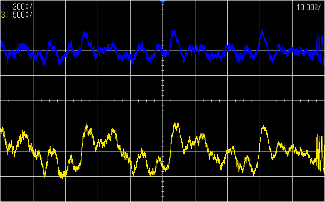
This shows the actual FM demodulated audio signal and which can be listened to with headphones plugged into the audio jack of the module. A recording of this, the demodulated audio output from the module, is presented below, it starts around the 30s mark. This uses the signal generator as the FM signal source:
And below is also a recording of the demodulated audio output from the module when using an FM Radio Station as the source, obtained connecting a VHF antenna to the module.
As already discussed in the AM demodulation section, the audio quality is not great and the majority of the loud and constant background noise is due to the way the transceivers DAC works and needs to be better suppressed with a better filter. The above results are with a double RC, second order, low pass filter. Besides this, further tuning and experimentation with the transceiver settings also promises to improve the FM demodulation and therefore the audio quality.
After revisiting the DAC output filtering, and looking up different low pass filter designs, a different low pass filter was tested, one that is compatible with the current hardware, a dual LC filter. For this the resistor of both RC filter stages are substituted with inductors which results in a two stage LC filter, second order filters, that effectively gives a forth order low pass filter. A comparison of the circuits and frequency responses of all the tested filters can be seen in the Hardware/Analog Output section.
Below is a figure that shows the filtered DAC output, in blue, when using the dual LC filter with a cutoff frequency of 23 kHz (L=22uH and C=2.2uF). Compared to the results above, when a dual RC filter was used, the noise reduction is visible. This is also noticeable when listening to the audio signal.
This filter needs further tuning as now the audio signal, although clearer with less noise, has a lower pitch/tone. This can be heard in the recording below, with the signal generator as the FM signal source:
The high frequency tone present in the signal is not present when listening trough headphones so it can be an artefact from the recording or it is filtered when using headphones, they are much lower impedance then the line in of a PC, which is used for the recording. Also, the improved audio quality in contrast to the recording with the RC filter is not all from changing the filter but also from the better way of recording the audio signal in general, with less peaking.
Results for NBFM
TBD
FM Audio Modulation
As seen in the FM Audio Demodulation section, analog FM is a unique and supported feature of the AX5043 transceiver and the same application note is used here as the basic guide. This section mirrors the configurations used for FM demodulation, same center frequency and using Wideband FM (WBFM).
The setup for FM Modulation is simpler then for the demodulation, as is the case with all modulations, and starts with setting up the ADC which is used to control the instantaneous frequency deviation. Here the ADC is used in differential mode, as seen in the Analog Input section, and therefore the ADC has to be set to use the GPADC13 input and continuous sampling mode. This is done by setting the GPADCCTRL (0x300) register to 0x06. Next the ADC sampling rate has to be set, this is done with the GPADCPERIOD (0x301) register, which has the following meaning:
$$ F_{Sample Rate} = { F_{XTAL} \over {32 * GPADCPERIOD} } $$
This sets the input signal sampling rate so how fast the frequency deviation is updated and therefore has to be set high enough for the desired application, over the Nyquist limit. For full definition audio, the commonly recommended sample rate is 44.1 kHz, while in the application note a sampling rate of 100 kHz is used. In my testing there was no noticeable difference in the transmitted audio quality for sample rates down to 25 kHz, other factors seem to be dominant until then.
Next, the maximum frequency deviation used has to be configured. For FM Modulation this is a scaling factor of the ADC value, how the ADC value is mapped to a frequency deviation, and is set with the FSKDEV (0x161-0x163) registers which has a different meaning in FM mode. The scaling is controlled by the FMSHIFT bits (bits 0-3) and have the following meaning:
$$ F_{Deviation} = { F_{XTAL} \over 2^{15 - FMSHIFT} } $$
This means that the maximum FM Deviations that can be used range from $ \pm 62.5 kHz $ down to $ \pm 488 Hz $. For WBFM, the highest frequency deviation is used by setting the FMSHIFT bits to 0x07. Next, the FMINPUT bits (bits 8-9) have to be set to 0x00, selecting the differential ADC channel (GPADC13) as the FM modulation source. Both the FMSEXT (bit 14) and FMOFFS (bit 15) bits should also be set so that differential ADC input generates both positive and negative frequency deviations.
With this, the only thing left is to enable continuous TX operation which is done by setting the PINFUNCDATA (0x023) register to 0x04, similar to wired mode but in FM mode no data is actually read from the DATA line. Finally, the transceiver is but into TX mode by setting the PWRMODE bits in the PWRMODE registers to 0x0D and with this the Wideband FM transmitter mode is configured and transmitting. A audio signal can now be injected to the Analog Input and this is then FM modulated and transmitted.
As seen in the Hardware section, the Analog Input circuit is responsible for converting the single ended AC coupled audio input to a differential signal with the correct scaling for the ADC input. The differential ADC input range is $ \pm 500mV $ with a common mode voltage of 800mV. This is done with a differential amplifier, the THS4521. Another differential amplifier was used first, the AD8137, but that one was not very stable in the used configuration/circuit, adding an oscillation on top of the signal.
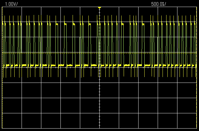
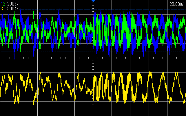
Below is a figure showing this conversion when applying a 500mVp-p 1kHz sine wave, shown in yellow, to the Analog Input. In green is the positive output and in blue the negative, the Analog Input uses the inverting amplifier circuit.
Below is a figure with an actual audio file as input, when using the full audio output range, 100% volume. Again, in yellow is the audio signal at the Analog Input and in green the positive output and blue the negative. It can be seen that with 100% volume, the output range is just inside the ADC input limits.
The transmitted signal spectrum when using a white noise audio file as the source/input is shown in the figure below, using the maximum PA output power. In yellow is the spectrum of this when using 100% volume which gives a full range ADC input, $ \pm 500mV $, and in red when using 50% volume which gives about a half range ADC input.
Because the FM Radio frequency range is used here, same as in the FM Audio Demodulation case, a normal FM Radio can be used to listen to the transmitted audio signal. Below is a recording of the transmitted audio signal, received and demodulated by my Smartphones FM receiver:
The audio quality is much better then expected, and when using headphones the sound quality is even better then what is shown in the recording. As seen above, the Analog Input circuit needs some improvements which should improve audio quality further.